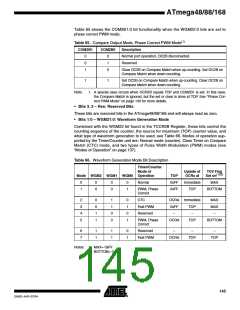
ATmega48/88/168
between OCR2x and TCNT2 when the counter decrements. The PWM frequency for the
output when using phase correct PWM can be calculated by the following equation:
f
clk_I/O
f
= -----------------
OCnxPCPWM
N ⋅ 510
The N variable represents the prescale factor (1, 8, 32, 64, 128, 256, or 1024).
The extreme values for the OCR2A Register represent special cases when generating a
PWM waveform output in the phase correct PWM mode. If the OCR2A is set equal to
BOTTOM, the output will be continuously low and if set equal to MAX the output will be
continuously high for non-inverted PWM mode. For inverted PWM the output will have
the opposite logic values.
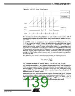
At the very start of period 2 in Figure 60 OCnx has a transition from high to low even
though there is no Compare Match. The point of this transition is to guarantee symmetry
around BOTTOM. There are two cases that give a transition without Compare Match.
•
OCR2A changes its value from MAX, like in Figure 60. When the OCR2A value is
MAX the OCn pin value is the same as the result of a down-counting compare
match. To ensure symmetry around BOTTOM the OCn value at MAX must
correspond to the result of an up-counting Compare Match.
•
The timer starts counting from a value higher than the one in OCR2A, and for that
reason misses the Compare Match and hence the OCn change that would have
happened on the way up.
Timer/Counter Timing
Diagrams
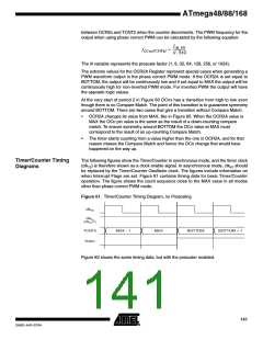
The following figures show the Timer/Counter in synchronous mode, and the timer clock
(clkT2) is therefore shown as a clock enable signal. In asynchronous mode, clkI/O should
be replaced by the Timer/Counter Oscillator clock. The figures include information on
when Interrupt Flags are set. Figure 61 contains timing data for basic Timer/Counter
operation. The figure shows the count sequence close to the MAX value in all modes
other than phase correct PWM mode.
Figure 61. Timer/Counter Timing Diagram, no Prescaling
clkI/O
clkTn
(clkI/O/1)
TCNTn
TOVn
MAX - 1
MAX
BOTTOM
BOTTOM + 1
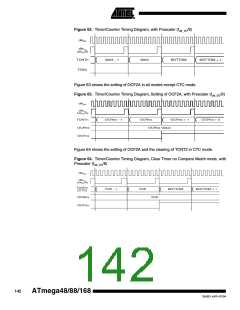
Figure 62 shows the same timing data, but with the prescaler enabled.
141
2545D–AVR–07/04

 ATMEL [ ATMEL ]