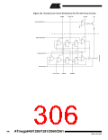
ATmega640/1280/1281/25 Table 131 shows the Scan order between TDI and TDO when the Boundary-scan chain
is selected as data path. Bit 0 is the LSB; the first bit scanned in, and the first bit
scanned out. The scan order follows the pin-out order as far as possible. Therefore, the
60/2561 Boundary-scan
Order
bits of Port A and Port K is scanned in the opposite bit order of the other ports. Excep-
tions from the rules are the Scan chains for the analog circuits, which constitute the
most significant bits of the scan chain regardless of which physical pin they are con-
nected to. In Figure 133, PXn. Data corresponds to FF0, PXn. Control corresponds to
FF1, PXn. Bit 4, 5, 6 and 7 of Port F is not in the scan chain, since these pins constitute
the TAP pins when the JTAG is enabled.
Table 131. ATmega640/1280/2560 Boundary-scan Order
Bit Number Signal Name
Module
164
163
162
161
160
159
158
157
156
155
154
153
152
151
150
149
148
147
146
145
144
143
142
141
140
139
138
137
136
PG5.Data
Port G
PG5.Control
PE0.Data
Port E
PE0.Control
PE1.Data
PE1.Control
PE2.Data
PE2.Control
PE3.Data
PE3.Control
PE4.Data
PE4.Control
PE5.Data
PE5.Control
PE6.Data
PE6.Control
PE7.Data
PE7.Control
PH0.Data
Port H
PH0.Control
PH1.Data
PH1.Control
PH2.Data
PH2.Control
PH3.Data
PH3.Control
PH4.Data
PH4.Control
PH5.Data
308
ATmega640/1280/1281/2560/2561
2549A–AVR–03/05

 ATMEL [ ATMEL ]