ATmega640/1280/1281/2560/2561
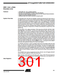
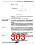
Figure 132. Reset Register
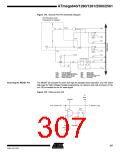
To
TDO
From Other Internal and
External Reset Sources
From
TDI
Internal reset
D
Q
ClockDR · AVR_RESET
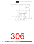
Boundary-scan Chain
The Boundary-scan Chain has the capability of driving and observing the logic levels on
the digital I/O pins, as well as the boundary between digital and analog logic for analog
circuitry having off-chip connections.
See “Boundary-scan Chain” on page 305 for a complete description.
Boundary-scan Specific The Instruction Register is 4-bit wide, supporting up to 16 instructions. Listed below are
the JTAG instructions useful for Boundary-scan operation. Note that the optional HIGHZ
JTAG Instructions
instruction is not implemented, but all outputs with tri-state capability can be set in high-
impedant state by using the AVR_RESET instruction, since the initial state for all port
pins is tri-state.
As a definition in this datasheet, the LSB is shifted in and out first for all Shift Registers.
The OPCODE for each instruction is shown behind the instruction name in hex format.
The text describes which Data Register is selected as path between TDI and TDO for
each instruction.
EXTEST; 0x0
Mandatory JTAG instruction for selecting the Boundary-scan Chain as Data Register for
testing circuitry external to the AVR package. For port-pins, Pull-up Disable, Output
Control, Output Data, and Input Data are all accessible in the scan chain. For Analog cir-
cuits having off-chip connections, the interface between the analog and the digital logic
is in the scan chain. The contents of the latched outputs of the Boundary-scan chain is
driven out as soon as the JTAG IR-Register is loaded with the EXTEST instruction.
The active states are:
•
•
•
Capture-DR: Data on the external pins are sampled into the Boundary-scan Chain.
Shift-DR: The Internal Scan Chain is shifted by the TCK input.
Update-DR: Data from the scan chain is applied to output pins.
IDCODE; 0x1
Optional JTAG instruction selecting the 32 bit ID-Register as Data Register. The ID-
Register consists of a version number, a device number and the manufacturer code
chosen by JEDEC. This is the default instruction after power-up.
The active states are:
•
Capture-DR: Data in the IDCODE Register is sampled into the Boundary-scan
Chain.
•
Shift-DR: The IDCODE scan chain is shifted by the TCK input.
303
2549A–AVR–03/05

 ATMEL [ ATMEL ]