ATmega640/1280/1281/2560/2561
8-bit Timer/Counter0 Timer/Counter0 is a general purpose 8-bit Timer/Counter module, with two independent
Output Compare Units, and with PWM support. It allows accurate program execution
timing (event management) and wave generation. The main features are:
• Two Independent Output Compare Units
with PWM
• Double Buffered Output Compare Registers
• Clear Timer on Compare Match (Auto Reload)
• Glitch Free, Phase Correct Pulse Width Modulator (PWM)
• Variable PWM Period
• Frequency Generator
• Three Independent Interrupt Sources (TOV0, OCF0A, and OCF0B)
Overview
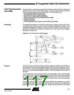
A simplified block diagram of the 8-bit Timer/Counter is shown in Figure 38. For the
actual placement of I/O pins, refer to “Pinout ATmega640/1280/2560” on page 2. CPU
accessible I/O Registers, including I/O bits and I/O pins, are shown in bold. The device-
specific I/O Register and bit locations are listed in the “8-bit Timer/Counter Register
Description” on page 128.
Figure 38. 8-bit Timer/Counter Block Diagram
Count
TOVn
(Int.Req.)
Clear
Control Logic
Clock Select
Direction
clkTn
Edge
Detector
Tn
TOP
BOTTOM
( From Prescaler )
Timer/Counter
TCNTn
=
= 0
OCnA
(Int.Req.)
Waveform
Generation
OCnA
OCnB
=
OCRnA
Fixed
TOP
Value
OCnB
(Int.Req.)
Waveform
Generation
=
OCRnB
TCCRnA
TCCRnB
Registers
The Timer/Counter (TCNT0) and Output Compare Registers (OCR0A and OCR0B) are
8-bit registers. Interrupt request (abbreviated to Int.Req. in the figure) signals are all vis-
ible in the Timer Interrupt Flag Register (TIFR0). All interrupts are individually masked
with the Timer Interrupt Mask Register (TIMSK0). TIFR0 and TIMSK0 are not shown in
the figure.
The Timer/Counter can be clocked internally, via the prescaler, or by an external clock
source on the T0 pin. The Clock Select logic block controls which clock source and edge
the Timer/Counter uses to increment (or decrement) its value. The Timer/Counter is
inactive when no clock source is selected. The output from the Clock Select logic is
referred to as the timer clock (clkT0).
The double buffered Output Compare Registers (OCR0A and OCR0B) are compared
with the Timer/Counter value at all times. The result of the compare can be used by the
Waveform Generator to generate a PWM or variable frequency output on the Output
117
2549A–AVR–03/05

 ATMEL [ ATMEL ]