26.9.15 Performing Chip Erase
1. Enter JTAG instruction PROG_COMMANDS.
2. Start Chip Erase using programming instruction 1a.
3. Poll for Chip Erase complete using programming instruction 1b, or wait for tWLRH_CE (refer
to Table 26-12 on page 308).
26.9.16 Programming the Flash
Before programming the Flash a Chip Erase must be performed, see “Performing Chip Erase”
on page 324.
1. Enter JTAG instruction PROG_COMMANDS.
2. Enable Flash write using programming instruction 2a.
3. Load address High byte using programming instruction 2b.
4. Load address Low byte using programming instruction 2c.
5. Load data using programming instructions 2d, 2e and 2f.
6. Repeat steps 4 and 5 for all instruction words in the page.
7. Write the page using programming instruction 2g.
8. Poll for Flash write complete using programming instruction 2h, or wait for tWLRH (refer to
Table 26-12 on page 308).
9. Repeat steps 3 to 7 until all data have been programmed.
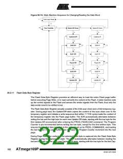
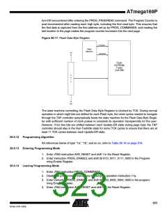
A more efficient data transfer can be achieved using the PROG_PAGELOAD instruction:
1. Enter JTAG instruction PROG_COMMANDS.
2. Enable Flash write using programming instruction 2a.
3. Load the page address using programming instructions 2b and 2c. PCWORD (refer to
Table 26-6 on page 298) is used to address within one page and must be written as 0.
4. Enter JTAG instruction PROG_PAGELOAD.
5. Load the entire page by shifting in all instruction words in the page byte-by-byte, starting
with the LSB of the first instruction in the page and ending with the MSB of the last
instruction in the page. Use Update-DR to copy the contents of the Flash Data Byte Reg-
ister into the Flash page location and to auto-increment the Program Counter before
each new word.
6. Enter JTAG instruction PROG_COMMANDS.
7. Write the page using programming instruction 2g.
8. Poll for Flash write complete using programming instruction 2h, or wait for tWLRH (refer to
Table 26-12 on page 308).
9. Repeat steps 3 to 8 until all data have been programmed.
324
ATmega169P
8018A–AVR–03/06

 ATMEL [ ATMEL ]