ATmega169P
6.3
EEPROM Data Memory
The ATmega169P contains 512 bytes of data EEPROM memory. It is organized as a separate
data space, in which single bytes can be read and written. The EEPROM has an endurance of at
least 100,000 write/erase cycles. This section describes the access between the EEPROM and
the CPU, specifying the EEPROM Address Registers, the EEPROM Data Register, and the
EEPROM Control Register.
For a detailed description of SPI, JTAG and Parallel data downloading to the EEPROM, see
”Serial Downloading” on page 309, ”Programming via the JTAG Interface” on page 314, and
”Parallel Programming Parameters, Pin Mapping, and Commands” on page 298 respectively.
6.3.1
EEPROM Read/Write Access
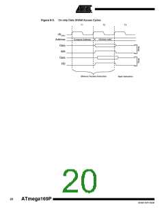
The EEPROM Access Registers are accessible in the I/O space.
The write access time for the EEPROM is given in Table 6-1 on page 22. A self-timing function,
however, lets the user software detect when the next byte can be written. If the user code con-
tains instructions that write the EEPROM, some precautions must be taken. In heavily filtered
power supplies, VCC is likely to rise or fall slowly on power-up/down. This causes the device for
some period of time to run at a voltage lower than specified as minimum for the clock frequency
used. See ”Preventing EEPROM Corruption” on page 25 for details on how to avoid problems in
these situations.
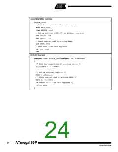
In order to prevent unintentional EEPROM writes, a specific write procedure must be followed.
When the EEPROM is read, the CPU is halted for four clock cycles before the next instruction is
executed. When the EEPROM is written, the CPU is halted for two clock cycles before the next
instruction is executed.
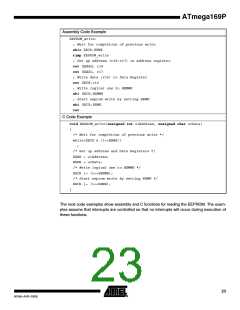
The following procedure should be followed when writing the EEPROM (the order of steps 3 and
4 is not essential). See ”EEPROM Register Description” on page 26 for supplementary descrip-
tion for each register bit:
1. Wait until EEWE becomes zero.
2. Wait until SPMEN in SPMCSR becomes zero.
3. Write new EEPROM address to EEAR (optional).
4. Write new EEPROM data to EEDR (optional).
5. Write a logical one to the EEMWE bit while writing a zero to EEWE in EECR.
6. Within four clock cycles after setting EEMWE, write a logical one to EEWE.
The EEPROM can not be programmed during a CPU write to the Flash memory. The software
must check that the Flash programming is completed before initiating a new EEPROM write.
Step 2 is only relevant if the software contains a Boot Loader allowing the CPU to program the
Flash. If the Flash is never being updated by the CPU, step 2 can be omitted. See ”Boot Loader
Support – Read-While-Write Self-Programming” on page 279 for details about Boot
programming.
Caution: An interrupt between step 5 and step 6 will make the write cycle fail, since the
EEPROM Master Write Enable will time-out. If an interrupt routine accessing the EEPROM is
interrupting another EEPROM access, the EEAR or EEDR Register will be modified, causing the
interrupted EEPROM access to fail. It is recommended to have the Global Interrupt Flag cleared
during all the steps to avoid these problems.
21
8018A–AVR–03/06

 ATMEL [ ATMEL ]