ATmega169P
6.2
SRAM Data Memory
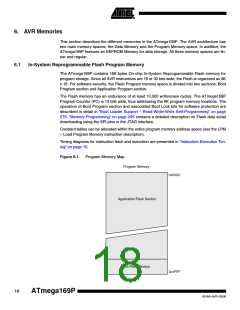
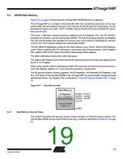
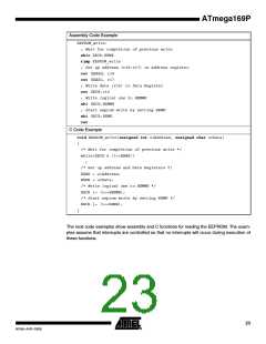
Figure 6-2 on page 19 shows how the ATmega169P SRAM Memory is organized.
The ATmega169P is a complex microcontroller with more peripheral units than can be sup-
ported within the 64 locations reserved in the Opcode for the IN and OUT instructions. For the
Extended I/O space from 0x60 - 0xFF in SRAM, only the ST/STS/STD and LD/LDS/LDD instruc-
tions can be used.
The lower 1,280 data memory locations address both the Register File, the I/O memory,
Extended I/O memory, and the internal data SRAM. The first 32 locations address the Register
File, the next 64 location the standard I/O memory, then 160 locations of Extended I/O memory,
and the next 1024 locations address the internal data SRAM.
The five different addressing modes for the data memory cover: Direct, Indirect with Displace-
ment, Indirect, Indirect with Pre-decrement, and Indirect with Post-increment. In the Register
File, registers R26 to R31 feature the indirect addressing pointer registers.
The direct addressing reaches the entire data space.
The Indirect with Displacement mode reaches 63 address locations from the base address given
by the Y- or Z-register.
When using register indirect addressing modes with automatic pre-decrement and post-incre-
ment, the address registers X, Y, and Z are decremented or incremented.
The 32 general purpose working registers, 64 I/O Registers, 160 Extended I/O Registers, and
the 1,024 bytes of internal data SRAM in the ATmega169P are all accessible through all these
addressing modes. The Register File is described in ”General Purpose Register File” on page
13.
Figure 6-2. Data Memory Map
Data Memory
0x0000 - 0x001F
0x0020 - 0x005F
0x0060 - 0x00FF
32 Registers
64 I/O Registers
160 Ext I/O Reg.
0x0100
Internal SRAM
(1024 x 8)
0x04FF
6.2.1
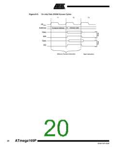
Data Memory Access Times
This section describes the general access timing concepts for internal memory access. The
internal data SRAM access is performed in two clkCPU cycles as described in Figure 6-3 on page
20.
19
8018A–AVR–03/06

 ATMEL [ ATMEL ]