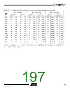
an interrupt when the transfer is complete. Note that when an external clock source is selected
the counter counts both clock edges. In this case the counter counts the number of edges, and
not the number of bits. The clock can be selected from three different sources: The USCK pin,
Timer/Counter0 Compare Match or from software.
The Two-wire clock control unit can generate an interrupt when a start condition is detected on
the Two-wire bus. It can also generate wait states by holding the clock pin low after a start con-
dition is detected, or after the counter overflows.
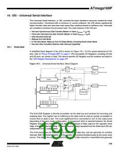
19.2 Functional Descriptions
19.2.1
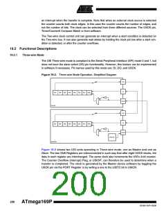
Three-wire Mode
The USI Three-wire mode is compliant to the Serial Peripheral Interface (SPI) mode 0 and 1, but
does not have the slave select (SS) pin functionality. However, this feature can be implemented
in software if necessary. Pin names used by this mode are: DI, DO, and USCK.
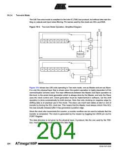
Figure 19-2. Three-wire Mode Operation, Simplified Diagram
DO
DI
Bit7
Bit6
Bit5
Bit4
Bit3
Bit2
Bit1
Bit0
USCK
SLAVE
DO
DI
Bit7
Bit6
Bit5
Bit4
Bit3
Bit2
Bit1
Bit0
USCK
PORTxn
MASTER
Figure 19-2 shows two USI units operating in Three-wire mode, one as Master and one as
Slave. The two Shift Registers are interconnected in such way that after eight USCK clocks, the
data in each register are interchanged. The same clock also increments the USI’s 4-bit counter.
The Counter Overflow (interrupt) Flag, or USIOIF, can therefore be used to determine when a
transfer is completed. The clock is generated by the Master device software by toggling the
USCK pin via the PORT Register or by writing a one to the USITC bit in USICR.
200
ATmega169P
8018A–AVR–03/06

 ATMEL [ ATMEL ]