ATmega169P
19. USI – Universal Serial Interface
The Universal Serial Interface, or USI, provides the basic hardware resources needed for serial
communication. Combined with a minimum of control software, the USI allows significantly
higher transfer rates and uses less code space than solutions based on software only. Interrupts
are included to minimize the processor load. The main features of the USI are:
• Two-wire Synchronous Data Transfer (Master or Slave, fSCLmax = fCK/16)
• Three-wire Synchronous Data Transfer (Master or Slave fSCKmax = fCK/4)
• Data Received Interrupt
• Wakeup from Idle Mode
• In Two-wire Mode: Wake-up from All Sleep Modes, Including Power-down Mode
• Two-wire Start Condition Detector with Interrupt Capability
19.1 Overview
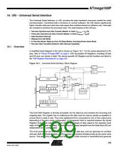
A simplified block diagram of the USI is shown on Figure 19-1. For the actual placement of I/O
pins, refer to ”Pinout ATmega169P” on page 2. CPU accessible I/O Registers, including I/O bits
and I/O pins, are shown in bold. The device-specific I/O Register and bit locations are listed in
the ”USI Register Descriptions” on page 207.
Figure 19-1. Universal Serial Interface, Block Diagram
(Output only)
DO
D
Q
LE
(Input/Open Drain)
DI/SDA
3
2
USIDR
1
0
TIM0 COMP
3
2
0
1
(Input/Open Drain)
USCK/SCL
4-bit Counter
1
0
CLOCK
HOLD
[1]
Two-wire Clock
Control Unit
USISR
2
USICR
The 8-bit Shift Register is directly accessible via the data bus and contains the incoming and
outgoing data. The register has no buffering so the data must be read as quickly as possible to
ensure that no data is lost. The most significant bit is connected to one of two output pins
depending of the wire mode configuration. A transparent latch is inserted between the Serial
Register Output and output pin, which delays the change of data output to the opposite clock
edge of the data input sampling. The serial input is always sampled from the Data Input (DI) pin
independent of the configuration.
The 4-bit counter can be both read and written via the data bus, and can generate an overflow
interrupt. Both the Serial Register and the counter are clocked simultaneously by the same clock
source. This allows the counter to count the number of bits received or transmitted and generate
199
8018A–AVR–03/06

 ATMEL [ ATMEL ]