ATmega169P
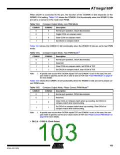
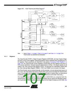
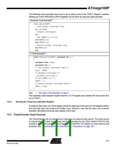
Figure 14-1. 16-bit Timer/Counter Block Diagram(1)
Count
TOVn
(Int.Req.)
Clear
Control Logic
Clock Select
Direction
clkTn
Edge
Detector
Tn
TOP
BOTTOM
( From Prescaler )
Timer/Counter
TCNTn
=
= 0
OCnA
(Int.Req.)
Waveform
Generation
OCnA
OCnB
=
OCRnA
OCnB
(Int.Req.)
Fixed
TOP
Values
Waveform
Generation
=
OCRnB
( From Analog
Comparator Ouput )
ICFn (Int.Req.)
Edge
Detector
Noise
Canceler
ICRn
ICPn
TCCRnA
TCCRnB
Note:
1. Refer to Figure 1-1 on page 2, Table 12-5 on page 74, and Table 12-11 on page 78 for
Timer/Counter1 pin placement and description.
14.1.1
Registers
The Timer/Counter (TCNT1), Output Compare Registers (OCR1A/B), and Input Capture Regis-
ter (ICR1) are all 16-bit registers. Special procedures must be followed when accessing the 16-
bit registers. These procedures are described in the section ”Accessing 16-bit Registers” on
page 109. The Timer/Counter Control Registers (TCCR1A/B) are 8-bit registers and have no
CPU access restrictions. Interrupt requests (abbreviated to Int.Req. in the figure) signals are all
visible in the Timer Interrupt Flag Register (TIFR1). All interrupts are individually masked with
the Timer Interrupt Mask Register (TIMSK1). TIFR1 and TIMSK1 are not shown in the figure.
The Timer/Counter can be clocked internally, via the prescaler, or by an external clock source on
the T1 pin. The Clock Select logic block controls which clock source and edge the Timer/Counter
uses to increment (or decrement) its value. The Timer/Counter is inactive when no clock source
is selected. The output from the Clock Select logic is referred to as the timer clock (clk ).
1
T
The double buffered Output Compare Registers (OCR1A/B) are compared with the
Timer/Counter value at all time. The result of the compare can be used by the Waveform Gener-
ator to generate a PWM or variable frequency output on the Output Compare pin (OC1A/B). See
107
8018A–AVR–03/06

 ATMEL [ ATMEL ]