ATmega128(L)
AVR USART vs. AVR
UART – Compatibility
The USART is fully compatible with the AVR UART regarding:
•
•
•
•
•
Bit locations inside all USART registers
Baud Rate Generation
Transmitter Operation
Transmit Buffer Functionality
Receiver Operation
However, the receive buffering has two improvements that will affect the compatibility in some
special cases:
•
A second buffer register has been added. The two buffer registers operate as a circular FIFO
buffer. Therefore the UDR must only be read once for each incoming data! More important is
the fact that the error flags (FE and DOR) and the ninth data bit (RXB8) are buffered with the
data in the receive buffer. Therefore the status bits must always be read before the UDR
Register is read. Otherwise the error status will be lost since the buffer state is lost.
•
The receiver Shift Register can now act as a third buffer level. This is done by allowing the
received data to remain in the serial Shift Register (see Figure 79) if the buffer registers are
full, until a new start bit is detected. The USART is therefore more resistant to Data OverRun
(DOR) error conditions.
The following control bits have changed name, but have same functionality and register location:
•
•
CHR9 is changed to UCSZ2
OR is changed to DOR
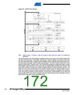
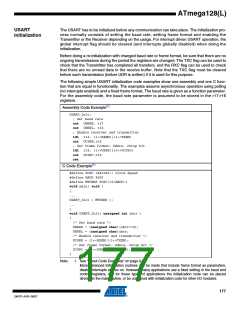
Clock Generation
The clock generation logic generates the base clock for the transmitter and receiver. The
USART supports four modes of clock operation: Normal Asynchronous, Double Speed Asyn-
chronous, Master Synchronous, and Slave Synchronous mode. The UMSEL bit in USART
Control and Status Register C (UCSRC) selects between asynchronous and synchronous oper-
ation. Double speed (Asynchronous mode only) is controlled by the U2X found in the UCSRA
Register. When using Synchronous mode (UMSEL = 1), the Data Direction Register for the XCK
pin (DDR_XCK) controls whether the clock source is internal (Master mode) or external (Slave
mode). The XCK pin is only active when using Synchronous mode.
Figure 80 shows a block diagram of the clock generation logic.
Figure 80. Clock Generation Logic, Block Diagram
UBRR
U2X
fosc
UBRR+1
Prescaling
Down-Counter
/ 2
/ 4
/ 2
0
1
0
1
OSC
txclk
UMSEL
rxclk
DDR_XCK
Sync
Register
Edge
Detector
xcki
0
1
XCK
Pin
xcko
DDR_XCK
UCPOL
1
0
Signal description:
173
2467P–AVR–08/07

 ATMEL [ ATMEL ]