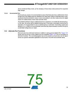
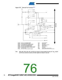
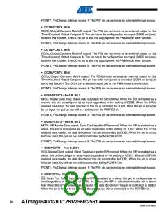
Figure 13-5. Alternate Port Functions(Note:)
PUOExn
PUOVxn
1
PUD
0
DDOExn
DDOVxn
1
Q
D
0
DDxn
Q CLR
WDx
RDx
PVOExn
PVOVxn
RESET
1
1
0
Pxn
Q
D
0
PORTxn
PTOExn
Q CLR
DIEOExn
WPx
DIEOVxn
RESET
WRx
1
RRx
0
SLEEP
SYNCHRONIZER
RPx
SET
D
Q
D
L
Q
Q
PINxn
CLR Q
CLR
clk I/O
DIxn
AIOxn
PUOExn: Pxn PULL-UP OVERRIDE ENABLE
PUOVxn: Pxn PULL-UP OVERRIDE VALUE
DDOExn: Pxn DATA DIRECTION OVERRIDE ENABLE
DDOVxn: Pxn DATA DIRECTION OVERRIDE VALUE
PVOExn: Pxn PORT VALUE OVERRIDE ENABLE
PVOVxn: Pxn PORT VALUE OVERRIDE VALUE
PUD:
WDx:
RDx:
RRx:
WRx:
RPx:
WPx:
PULLUP DISABLE
WRITE DDRx
READ DDRx
READ PORTx REGISTER
WRITE PORTx
READ PORTx PIN
WRITE PINx
DIEOExn: Pxn DIGITAL INPUT-ENABLE OVERRIDE ENABLE
DIEOVxn: Pxn DIGITAL INPUT-ENABLE OVERRIDE VALUE
clkI/O
:
I/O CLOCK
SLEEP:
SLEEP CONTROL
DIxn:
DIGITAL INPUT PIN n ON PORTx
AIOxn:
ANALOG INPUT/OUTPUT PIN n ON PORTx
PTOExn: Pxn, PORT TOGGLE OVERRIDE ENABLE
Note:
WRx, WPx, WDx, RRx, RPx, and RDx are common to all pins within the same port. clkI/O, SLEEP,
and PUD are common to all ports. All other signals are unique for each pin.
76
ATmega640/1280/1281/2560/2561
2549L–AVR–08/07

 ATMEL [ ATMEL ]