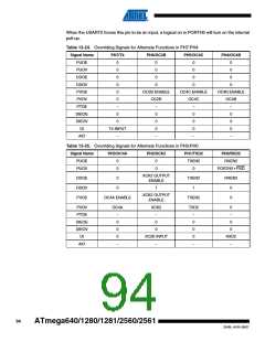
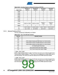
Table 13-29. Overriding Signals for Alternate Functions in PK3:PK0
PK3/ADC11/
PCINT19
PK2/ADC10/
PCINT18
PK1/ADC9/
PCINT17
PK0/ADC8/
PCINT16
Signal Name
PUOE
0
0
0
0
0
0
–
0
0
0
0
0
0
–
0
0
0
0
0
0
–
0
0
0
0
0
0
–
PUOV
DDOE
DDOV
PVOE
PVOV
PTOE
PCINT17 •
PCIE2
PCINT16 •
PCIE2
DIEOE
PCINT19 • PCIE2
PCINT18 • PCIE2
DIEOV
DI
1
1
1
1
PCINT19 INPUT
ADC11 INPUT
PCINT18 INPUT
ADC10INPUT
PCINT17 INPUT PCINT16 INPUT
ADC9 INPUT ADC8 INPUT
AIO
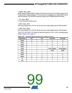
13.3.11 Alternate Functions of Port L
The Port L alternate pin configuration is as follows:
Table 13-30. Port L Pins Alternate Functions
Port Pin
PL7
Alternate Function
–
–
PL6
PL5
OC5C (Output Compare and PWM Output C for Timer/Counter5)
OC5B (Output Compare and PWM Output B for Timer/Counter5)
OC5A (Output Compare and PWM Output A for Timer/Counter5)
T5 (Timer/Counter5 Clock Input)
PL4
PL3
PL2
PL1
ICP5 (Timer/Counter5 Input Capture Trigger)
PL0
ICP4 (Timer/Counter4 Input Capture Trigger)
• OC5C – Port L, Bit 5
OC5C, Output Compare Match C output: The PL5 pin can serve as an external output for the
Timer/Counter5 Output Compare C. The pin has to be configured as an output (DDL5 set) to
serve this function. The OC5C pin is also the output pin for the PWM mode timer function.
• OC5B – Port L, Bit 4
OC5B, Output Compare Match B output: The PL4 pin can serve as an external output for the
Timer/Counter 5 Output Compare B. The pin has to be configured as an output (DDL4 set) to
serve this function. The OC5B pin is also the output pin for the PWM mode timer function.
98
ATmega640/1280/1281/2560/2561
2549L–AVR–08/07

 ATMEL [ ATMEL ]