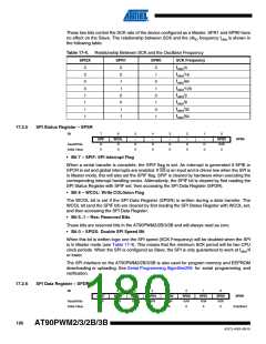
These two bits control the SCK rate of the device configured as a Master. SPR1 and SPR0 have
no effect on the Slave. The relationship between SCK and the clkIO frequency fclkio is shown in
the following table:
Table 17-4. Relationship Between SCK and the Oscillator Frequency
SPI2X
SPR1
SPR0
SCK Frequency
fclkio/4
0
0
0
0
1
1
1
1
0
0
1
1
0
0
1
1
0
1
0
1
0
1
0
1
fclkio/16
fclkio/64
fclkio/128
fclkio/2
fclkio/8
fclkio/32
fclkio/64
17.2.5
SPI Status Register – SPSR
Bit
7
SPIF
R
6
5
–
4
–
3
–
2
–
1
–
0
SPI2X
R/W
0
WCOL
SPSR
Read/Write
Initial Value
R
0
R
0
R
0
R
0
R
0
R
0
0
• Bit 7 – SPIF: SPI Interrupt Flag
When a serial transfer is complete, the SPIF flag is set. An interrupt is generated if SPIE in
SPCR is set and global interrupts are enabled. If SS is an input and is driven low when the SPI is
in Master mode, this will also set the SPIF flag. SPIF is cleared by hardware when executing the
corresponding interrupt handling vector. Alternatively, the SPIF bit is cleared by first reading the
SPI Status Register with SPIF set, then accessing the SPI Data Register (SPDR).
• Bit 6 – WCOL: Write COLlision Flag
The WCOL bit is set if the SPI Data Register (SPDR) is written during a data transfer. The
WCOL bit (and the SPIF bit) are cleared by first reading the SPI Status Register with WCOL set,
and then accessing the SPI Data Register.
• Bit 5..1 – Res: Reserved Bits
These bits are reserved bits in the AT90PWM2/2B/3/3B and will always read as zero.
• Bit 0 – SPI2X: Double SPI Speed Bit
When this bit is written logic one the SPI speed (SCK Frequency) will be doubled when the SPI
is in Master mode (see Table 17-4). This means that the minimum SCK period will be two CPU
clock periods. When the SPI is configured as Slave, the SPI is only guaranteed to work at fclkio/4
or lower.
The SPI interface on the AT90PWM2/2B/3/3B is also used for program memory and EEPROM
downloading or uploading. See Serial Programming Algorithm294 for serial programming and
verification.
17.2.6
SPI Data Register – SPDR
Bit
7
SPD7
R/W
X
6
SPD6
R/W
X
5
SPD5
R/W
X
4
SPD4
R/W
X
3
SPD3
R/W
X
2
SPD2
R/W
X
1
SPD1
R/W
X
0
SPD0
R/W
X
SPDR
Read/Write
Initial Value
Undefined
180
AT90PWM2/3/2B/3B
4317J–AVR–08/10

 ATMEL [ ATMEL ]