AT89S52
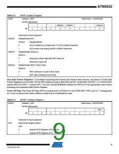
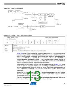
Table 5-3.
AUXR: Auxiliary Register
Address = 8EH
AUXR
Reset Value = XXX00XX0B
Not Bit Addressable
–
7
–
–
5
WDIDLE
4
DISRTO
3
–
2
–
1
DISALE
0
Bit
6
–
Reserved for future expansion
Disable/Enable ALE
DISALE
DISALE
Operating Mode
0
1
ALE is emitted at a constant rate of 1/6 the oscillator frequency
ALE is active only during a MOVX or MOVC instruction
DISRTO
WDIDLE
Disable/Enable Reset out
DISRTO
0
1
Reset pin is driven High after WDT times out
Reset pin is input only
Disable/Enable WDT in IDLE mode
WDIDLE
0
1
WDT continues to count in IDLE mode
WDT halts counting in IDLE mode
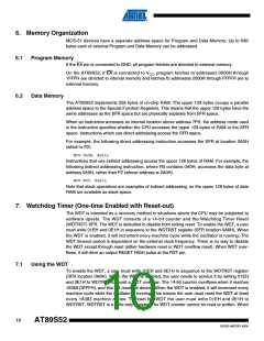
Dual Data Pointer Registers: To facilitate accessing both internal and external data memory, two banks of 16-bit Data
Pointer Registers are provided: DP0 at SFR address locations 82H-83H and DP1 at 84H-85H. Bit DPS = 0 in SFR AUXR1
selects DP0 and DPS = 1 selects DP1. The user should ALWAYS initialize the DPS bit to the appropriate value before
accessing the respective Data Pointer Register.
Power Off Flag: The Power Off Flag (POF) is located at bit 4 (PCON.4) in the PCON SFR. POF is set to “1” during power
up. It can be set and rest under software control and is not affected by reset.
Table 5-4.
AUXR1: Auxiliary Register 1
Address = A2H
AUXR1
Reset Value = XXXXXXX0B
Not Bit Addressable
–
7
–
6
–
5
–
4
–
3
–
2
–
1
DPS
0
Bit
–
Reserved for future expansion
Data Pointer Register Select
DPS
DPS
0
1
Selects DPTR Registers DP0L, DP0H
Selects DPTR Registers DP1L, DP1H
9
1919D–MICRO–6/08

 ATMEL [ ATMEL ]