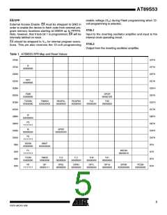
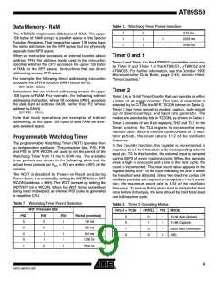
Pin Configurations
PDIP
PLCC
(T2) P1.0
(T2 EX) P1.1
P1.2
1
2
3
4
5
6
7
8
9
40 VCC
39 P0.0 (AD0)
38 P0.1 (AD1)
37 P0.2 (AD2)
36 P0.3 (AD3)
35 P0.4 (AD4)
34 P0.5 (AD5)
33 P0.6 (AD6)
32 P0.7 (AD7)
31 EA/VPP
P1.3
(SS) P1.4
(MOSI) P1.5
(MISO) P1.6
(SCK) P1.7
RST
(MOSI) P1.5
(MISO) P1.6
(SCK) P1.7
7
8
9
39 P0.4 (AD4)
38 P0.5 (AD5)
37 P0.6 (AD6)
36 P0.7 (AD7)
35 EA/VPP
RST 10
(RXD) P3.0 11
NC 12
(RXD) P3.0 10
(TXD) P3.1 11
(INT0) P3.2 12
(INT1) P3.3 13
(T0) P3.4 14
(T1) P3.5 15
(WR) P3.6 16
(RD) P3.7 17
XTAL2 18
30 ALE/PROG
29 PSEN
34 NC
(TXD) P3.1 13
(INT0) P3.2 14
(INT1) P3.3 15
(T0) P3.4 16
(T1) P3.5 17
33 ALE/PROG
32 PSEN
28 P2.7 (A15)
27 P2.6 (A14)
26 P2.5 (A13)
25 P2.4 (A12)
24 P2.3 (A11)
23 P2.2 (A10)
22 P2.1 (A9)
21 P2.0 (A8)
31 P2.7 (A15)
30 P2.6 (A14)
29 P2.5 (A13)
XTAL1 19
GND 20
TQFP
(MOSI) P1.5
(MISO) P1.6
(SCK) P1.7
RST
1
2
3
4
5
6
7
8
9
33 P0.4 (AD4)
32 P0.5 (AD5)
31 P0.6 (AD6)
30 P0.7 (AD7)
29 EA/VPP
28 NC
(RXD) P3.0
NC
(TXD) P3.1
(INT0) P3.2
(INT1) P3.3
27 ALE/PROG
26 PSEN
25 P2.7 (A15)
24 P2.6 (A14)
23 P2.5 (A13)
(T0) P3.4 10
(T1) P3.5 11
Port 0 can also be configured to be the multiplexed low-
order address/data bus during accesses to external
program and data memory. In this mode, P0 has internal
pullups.
Pin Description
VCC
Supply voltage.
Port 0 also receives the code bytes during Flash program-
ming and outputs the code bytes during program
verification. External pullups are required during program
verification.
GND
Ground.
Port 0
Port 1
Port 0 is an 8-bit open drain bidirectional I/O port. As an
output port, each pin can sink eight TTL inputs. When 1s
are written to port 0 pins, the pins can be used as high-
impedance inputs.
Port 1 is an 8-bit bidirectional I/O port with internal pullups.
The Port 1 output buffers can sink/source four TTL inputs.
When 1s are written to Port 1 pins, they are pulled high by
the internal pullups and can be used as inputs. As inputs,
Port 1 pins that are externally being pulled low will source
current (IIL) because of the internal pullups.
2
AT89S53
0787E–MICRO–3/06

 ATMEL [ ATMEL ]