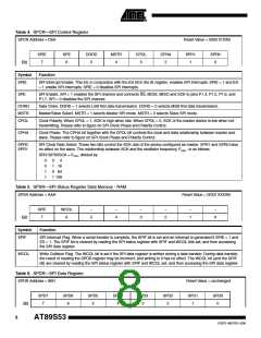
Table 4. SPCR—SPI Control Register
SPCR Address = D5H
Reset Value = 0000 01XXB
SPIE
7
SPE
6
DORD
5
MSTR
4
CPOL
3
CPHA
2
SPR1
1
SPR0
0
Bit
Symbol
Function
SPIE
SPI Interrupt Enable. This bit, in conjunction with the ES bit in the IE register, enables SPI interrupts: SPIE = 1 and ES
= 1 enable SPI interrupts. SPIE = 0 disables SPI interrupts.
SPE
SPI Enable. SPI = 1 enables the SPI channel and connects SS, MOSI, MISO and SCK to pins P1.4, P1.5, P1.6, and
P1.7. SPI = 0 disables the SPI channel.
DORD
MSTR
CPOL
Data Order. DORD = 1 selects LSB first data transmission. DORD = 0 selects MSB first data transmission.
Master/Slave Select. MSTR = 1 selects Master SPI mode. MSTR = 0 selects Slave SPI mode.
Clock Polarity. When CPOL = 1, SCK is high when idle. When CPOL = 0, SCK of the master device is low when not
transmitting. Please refer to figure on SPI Clock Phase and Polarity Control.
CPHA
Clock Phase. The CPHA bit together with the CPOL bit controls the clock and data relationship between master and
slave. Please refer to figure on SPI Clock Phase and Polarity Control.
SPR0
SPR1
SPI Clock Rate Select. These two bits control the SCK rate of the device configured as master. SPR1 and SPR0 have
no effect on the slave. The relationship between SCK and the oscillator frequency, FOSC., is as follows:
SPR1SPR0SCK = FOSC. divided by
0
0
1
1
0
1
0
4
16
64
1 128
Table 5. SPSR—SPI Status Register Data Memory - RAM
SPSR Address = AAH
Reset Value = 00XX XXXXB
SPIF
7
WCOL
6
–
5
–
4
–
3
–
2
–
1
–
0
Bit
Symbol
Function
SPIF
SPI Interrupt Flag. When a serial transfer is complete, the SPIF bit is set and an interrupt is generated if SPIE = 1 and
ES = 1. The SPIF bit is cleared by reading the SPI status register with SPIF and WCOL bits set, and then accessing
the SPI data register.
WCOL
Write Collision Flag. The WCOL bit is set if the SPI data register is written during a data transfer. During data transfer,
the result of reading the SPDR register may be incorrect, and writing to it has no effect. The WCOL bit (and the SPIF
bit) are cleared by reading the SPI status register with SPIF and WCOL set, and then accessing the SPI data register.
Table 6. SPDR—SPI Data Register
SPDR Address = 86H
Reset Value = unchanged
SPD7
7
SPD6
6
SPD5
5
SPD4
4
SPD3
3
SPD2
2
SPD1
1
SPD0
0
Bit
8
AT89S53
0787E–MICRO–3/06

 ATMEL [ ATMEL ]