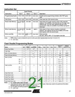
AT89S53
Timer 2 interrupt is generated by the logical OR of bits TF2
and EXF2 in register T2CON. Neither of these flags is
cleared by hardware when the service routine is vectored
to. In fact, the service routine may have to determine
whether it was TF2 or EXF2 that generated the interrupt,
and that bit will have to be cleared in software.
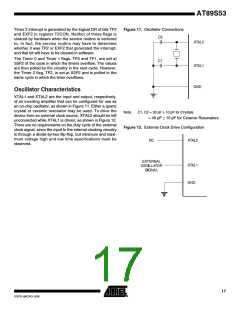
Figure 11. Oscillator Connections
The Timer 0 and Timer 1 flags, TF0 and TF1, are set at
S5P2 of the cycle in which the timers overflow. The values
are then polled by the circuitry in the next cycle. However,
the Timer 2 flag, TF2, is set at S2P2 and is polled in the
same cycle in which the timer overflows.
Oscillator Characteristics
XTAL1 and XTAL2 are the input and output, respectively,
of an inverting amplifier that can be configured for use as
an on-chip oscillator, as shown in Figure 11. Either a quartz
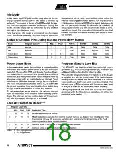
crystal or ceramic resonator may be used. To drive the
device from an external clock source, XTAL2 should be left
unconnected while XTAL1 is driven, as shown in Figure 12.
There are no requirements on the duty cycle of the external
clock signal, since the input to the internal clocking circuitry
is through a divide-by-two flip-flop, but minimum and maxi-
mum voltage high and low time specifications must be
observed.
Note:
C1, C2 = 30 pF ± 10 pF for Crystals
= 40 pF ± 10 pF for Ceramic Resonators
Figure 12. External Clock Drive Configuration
17
0787E–MICRO–3/06

 ATMEL [ ATMEL ]