AT89S53
• Write Collision Flag Protection
UART
• Wakeup from Idle Mode (Slave Mode Only)
The UART in the AT89S53 operates the same way as the
UART in the AT89C51, AT89C52 and AT89C55. For fur-
ther information, see the October 1995 Microcontroller
Data Book, page 2-49, section titled, “Serial Interface.”
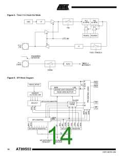
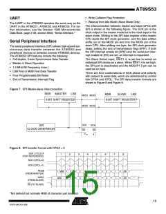
The interconnection between master and slave CPUs with
SPI is shown in the following figure. The SCK pin is the
clock output in the master mode but is the clock input in the
slave mode. Writing to the SPI data register of the master
CPU starts the SPI clock generator, and the data written
shifts out of the MOSI pin and into the MOSI pin of the
slave CPU. After shifting one byte, the SPI clock generator
stops, setting the end of transmission flag (SPIF). If both
the SPI interrupt enable bit (SPIE) and the serial port inter-
rupt enable bit (ES) are set, an interrupt is requested.
Serial Peripheral Interface
The serial peripheral interface (SPI) allows high-speed syn-
chronous data transfer between the AT89S53 and
peripheral devices or between several AT89S53 devices.
The AT89S53 SPI features include the following:
• Full-duplex, 3-wire Synchronous Data Transfer
The Slave Select input, SS/P1.4, is set low to select an
individual SPI device as a slave. When SS/P1.4 is set high,
the SPI port is deactivated and the MOSI/P1.5 pin can be
used as an input.
• Master or Slave Operation
• 1.5 MHz Bit Frequency (max.)
• LSB First or MSB First Data Transfer
• Four Programmable Bit Rates
• End of Transmission Interrupt Flag
There are four combinations of SCK phase and polarity
with respect to serial data, which are determined by control
bits CPHA and CPOL. The SPI data transfer formats are
shown in Figure 8 and Figure 9.
Figure 7. SPI Master-slave Interconnection
MSB
MASTER
LSB
MSB
SLAVE
LSB
MISO MISO
MOSI MOSI
8-BIT SHIFT REGISTER
8-BIT SHIFT REGISTER
SCK
SS
SCK
SS
SPI
CLOCK GENERATOR
VCC
Figure 8. SPI transfer Format with CPHA = 0
*Not defined but normally MSB of character just received
15
0787E–MICRO–3/06

 ATMEL [ ATMEL ]