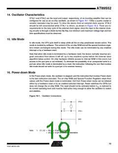
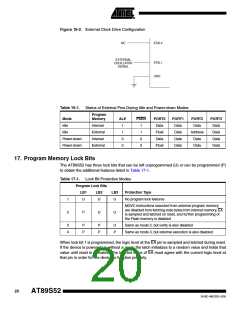
AT89S52
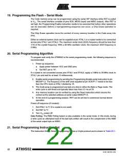
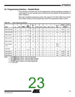
22. Programming Interface – Parallel Mode
Every code byte in the Flash array can be programmed by using the appropriate combination of
control signals. The write operation cycle is self-timed and once initiated, will automatically time
itself to completion.
Most major worldwide programming vendors offer support for the Atmel AT89 microcontroller
series. Please contact your local programming vendor for the appropriate software revision.
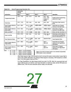
Table 22-1. Flash Programming Modes
P2.4-0
P1.7-0
ALE/
EA/
VPP
P0.7-0
Data
Address
Mode
VCC
5V
5V
5V
RST
H
PSEN
PROG
P2.6
P2.7
H
P3.3
H
P3.6
H
P3.7
H
(2)
Write Code Data
Read Code Data
Write Lock Bit 1
L
L
L
12V
H
L
L
DIN
DOUT
X
A12-8
A12-8
X
A7-0
A7-0
X
H
H
L
L
H
H
(3)
H
12V
H
H
H
H
H
(3)
(3)
Write Lock Bit 2
Write Lock Bit 3
5V
5V
H
H
L
L
12V
12V
H
H
H
L
H
H
L
L
L
X
X
X
X
X
X
H
P0.2,
P0.3,
P0.4
Read Lock Bits
1, 2, 3
5V
5V
H
H
L
L
H
H
H
H
H
L
L
H
L
L
L
X
X
X
X
(1)
Chip Erase
12V
H
X
Read Atmel ID
Read Device ID
Read Device ID
5V
5V
5V
H
H
H
L
L
L
H
H
H
H
H
H
L
L
L
L
L
L
L
L
L
L
L
L
L
L
L
1EH
52H
06H
X 0000
X 0001
X 0010
00H
00H
00H
Notes: 1. Each PROG pulse is 200 ns - 500 ns for Chip Erase.
2. Each PROG pulse is 200 ns - 500 ns for Write Code Data.
3. Each PROG pulse is 200 ns - 500 ns for Write Lock Bits.
4. RDY/BSY signal is output on P3.0 during programming.
5. X = don’t care.
23
1919C–MICRO–3/05

 ATMEL [ ATMEL ]