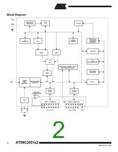
AT89C2051x2
Pin Description
VCC
Supply voltage.
Ground.
GND
Port 1
Port 1 is an 8-bit bi-directional I/O port. Port pins P1.2 to P1.7 provide internal pull-ups.
P1.0 and P1.1 require external pull-ups. P1.0 and P1.1 also serve as the positive input
(AIN0) and the negative input (AIN1), respectively, of the on-chip precision analog com-
parator. The Port 1 output buffers can sink 20 mA and can drive LED displays directly.
When 1s are written to Port 1 pins, they can be used as inputs. When pins P1.2 to P1.7
are used as inputs and are externally pulled low, they will source current (IIL) because of
the internal pull-ups.
Port 1 also receives code data during Flash programming and verification.
Port 3
Port 3 pins P3.0 to P3.5, P3.7 are seven bi-directional I/O pins with internal pull-ups.
P3.6 is hard-wired as an input to the output of the on-chip comparator and is not acces-
sible as a general purpose I/O pin. The Port 3 output buffers can sink 20 mA. When 1s
are written to Port 3 pins they are pulled high by the internal pull-ups and can be used as
inputs. As inputs, Port 3 pins that are externally being pulled low will source current (IIL)
because of the pull-ups.
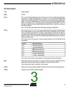
Port 3 also serves the functions of various special features of the AT89C2051x2 as
listed below:
Port Pin
P3.0
Alternate Functions
RXD (serial input port)
TXD (serial output port)
INT0 (external interrupt 0)
INT1 (external interrupt 1)
T0 (timer 0 external input)
T1 (timer 1 external input)
P3.1
P3.2
P3.3
P3.4
P3.5
Port 3 also receives some control signals for Flash programming and verification.
RST
Reset input. All I/O pins are reset to 1s as soon as RST goes high. Holding the RST pin
high for two machine cycles while the oscillator is running resets the device.
Each machine cycle takes 6 oscillator or clock cycles.
XTAL1
XTAL2
Input to the inverting oscillator amplifier and input to the internal clock operating circuit.
Output from the inverting oscillator amplifier.
3
3285B–MICRO–10/03

 ATMEL [ ATMEL ]