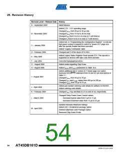
28. Revision History
Revision Level – Release Date History
A – September 2005
B – November 2005
Initial Release
Added 2.5V - 3.6V operating range.
Changed tVCSL from 30 µs to 50 µs min.
Changed tPUW from 10 ms to 20 ms max.
Changed tDIS from 8 ns to 6 ns max (2.7-volt device).
Changed tV from 8 ns to 6 ns max (2.7-volt device).
Added text, in “Programming the Configuration Register”, to indicate
that power cycling is required to switch to “power of 2” page size
after the opcode enable has been executed.
C – January 2006
Added “Legacy Commands” table.
D – February 2006
E – May 2006
Changed part 2 of the device ID to 00H.
Added Legacy Status Register Read opcode 57H. This opcode is
supported on devices with date code 0636 and later.
F – July 2006
Corrected typographical errors.
G – August 2006
H – August 2006
Added errata regarding Chip Erase.
Added tSCKR and tSCKF parameters to Table 18-4.
Added additional text to “power of 2” binary page size option.
Removed SER/BYTE statement from SI and SO pin descriptions in
Table 2-1.
I – August 2007
Changed tVSCL from 50 µs to 70 µs.
Changed tXFR and tCOMP values from 400 µs to 200 µs.
Changed tRDPD from 30 µs to 35 µs.
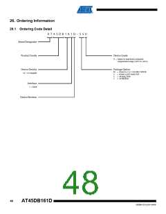
Added part number ordering code details for suffixes SL954/955.
Added ordering code details.
J – April 2008
K – February 2009
Changed tDIS (Typ and Max) to 27 ns and 35 ns, respectively.
Changed Deep Power-Down Current values
- Increased typical value from 5 µA to 15 µA.
- Increased maximum value from 15 µA to 25 µA.
L – March 2009
M - April 2009
Updated Absolute Maximum Ratings
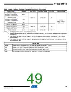
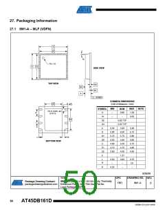
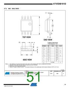
Added 24C1 24 Ball BGA package Option
Deleted DataFlash Card Package Option
Removed Chip Erase Errata
54
AT45DB161D
3500M–DFLASH–04/09

 ATMEL [ ATMEL ]