AT45DB161D
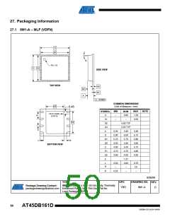
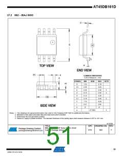
27.2 8S2 – EIAJ SOIC
C
1
E
E1
L
N
θ
TOP VIEW
ENDD VVIIEEWW
e
b
COMMON DIMENSIONS
(Unit of Measure = mm)
A
MIN
1.70
0.05
0.35
0.15
5.13
5.18
7.70
0.51
0°
MAX
2.16
0.25
0.48
0.35
5.35
5.40
8.26
0.85
8°
NOM
NOTE
SYMBOL
A1
A
A1
b
4
4
C
D
E1
E
D
2
L
SIDE VIEW
θ
e
1.27 BSC
3
Notes: 1. This drawing is for general information only; refer to EIAJ Drawing EDR-7320 for additional information.
2. Mismatch of the upper and lower dies and resin burrs aren't included.
3. Determines the true geometric position.
4. Values b,C apply to plated terminal. The standard thickness of the plating layer shall measure between 0.007 to .021 mm.
4/15/08
GPC
DRAWING NO.
TITLE
REV.
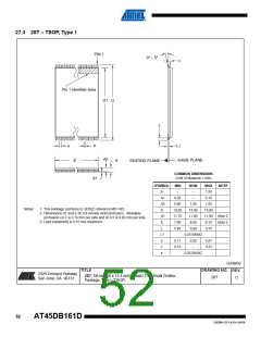
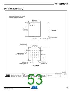
8S2, 8-lead, 0.208” Body, Plastic Small
Outline Package (EIAJ)
Package Drawing Contact:
packagedrawings@atmel.com
STN
8S2
F
51
3500M–DFLASH–04/09

 ATMEL [ ATMEL ]