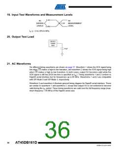
19. Input Test Waveforms and Measurement Levels
2.4V
AC
AC
DRIVING
LEVELS
1.5V
MEASUREMENT
LEVEL
0.45V
tR, tF < 2 ns (10% to 90%)
20. Output Test Load
DEVICE
UNDER
TEST
30 pF
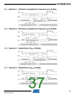
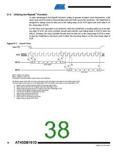
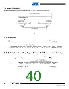
21. AC Waveforms
Six different timing waveforms are shown on page 37. Waveform 1 shows the SCK signal being
low when CS makes a high-to-low transition, and waveform 2 shows the SCK signal being high
when CS makes a high-to-low transition. In both cases, output SO becomes valid while the
SCK signal is still low (SCK low time is specified as tWL). Timing waveforms 1 and 2 conform to
RapidS serial interface but for frequencies up to 66 MHz. Waveforms 1 and 2 are compatible
with SPI Mode 0 and SPI Mode 3, respectively.
Waveform 3 and waveform 4 illustrate general timing diagram for RapidS serial interface. These
are similar to waveform 1 and waveform 2, except that output SO is not restricted to become
valid during the tWL period. These timing waveforms are valid over the full frequency range (max-
imum frequency = 66 MHz) of the RapidS serial case.
36
AT45DB161D
3500M–DFLASH–04/09

 ATMEL [ ATMEL ]