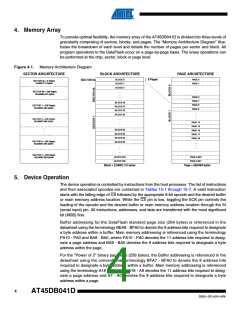
4. Memory Array
To provide optimal flexibility, the memory array of the AT45DB041D is divided into three levels of
granularity comprising of sectors, blocks, and pages. The “Memory Architecture Diagram” illus-
trates the breakdown of each level and details the number of pages per sector and block. All
program operations to the DataFlash occur on a page-by-page basis. The erase operations can
be performed at the chip, sector, block or page level.
Figure 4-1. Memory Architecture Diagram
SECTOR ARCHITECTURE
BLOCK ARCHITECTURE
PAGE ARCHITECTURE
BLOCK 0
BLOCK 1
BLOCK 2
8 Pages
PAGE 0
PAGE 1
SECTOR 0a
SECTOR 0a = 8 Pages
2,048/2,112 bytes
SECTOR 0b = 248 Pages
63,488/65,472 bytes
PAGE 6
PAGE 7
PAGE 8
PAGE 9
BLOCK 30
BLOCK 31
BLOCK 32
BLOCK 33
SECTOR 1 = 256 Pages
65,536/67,584 bytes
SECTOR 2 = 256 Pages
65,536/67,584 bytes
PAGE 14
PAGE 15
PAGE 16
PAGE 17
PAGE 18
BLOCK 62
BLOCK 63
BLOCK 64
BLOCK 65
SECTOR 6 = 256 Pages
65,536/67,584 bytes
SECTOR 7 = 256 Pages
65,536/67,584 bytes
BLOCK 254
BLOCK 255
PAGE 2,046
PAGE 2,047
Block = 2,048/2,112 bytes
Page = 256/264 bytes
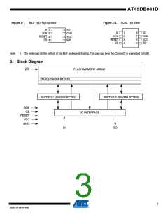
5. Device Operation
The device operation is controlled by instructions from the host processor. The list of instructions
and their associated opcodes are contained in Tables 15-1 through 15-7. A valid instruction
starts with the falling edge of CS followed by the appropriate 8-bit opcode and the desired buffer
or main memory address location. While the CS pin is low, toggling the SCK pin controls the
loading of the opcode and the desired buffer or main memory address location through the SI
(serial input) pin. All instructions, addresses, and data are transferred with the most significant
bit (MSB) first.
Buffer addressing for the DataFlash standard page size (264 bytes) is referenced in the
datasheet using the terminology BEA8 - BFA0 to denote the 9 address bits required to designate
a byte address within a buffer. Main memory addressing is referenced using the terminology
PA10 - PA0 and BA8 - BA0, where PA10 - PA0 denotes the 11 address bits required to desig-
nate a page address and BA8 - BA0 denotes the 9 address bits required to designate a byte
address within the page.
For the “Power of 2” binary page size (256 bytes), the Buffer addressing is referenced in the
datasheet using the conventional terminology BFA7 - BFA0 to denote the 8 address bits
required to designate a byte address within a buffer. Main memory addressing is referenced
using the terminology A18 - A0, where A18 - A8 denotes the 11 address bits required to desig-
nate a page address and A7 - A0 denotes the 8 address bits required to designate a byte
address within a page.
4
AT45DB041D
3595L–DFLASH–4/08

 ATMEL [ ATMEL ]