increases system reliability, minimizes switching noise, and reduces package size. The device is
optimized for use in many commercial and industrial applications where high-density, low-pin
count, low-voltage and low-power are essential.
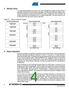
To allow for simple in-system reprogrammability, the AT45DB041D does not require high input
voltages for programming. The device operates from a single power supply, 2.5V to 3.6V or 2.7V
to 3.6V, for both the program and read operations. The AT45DB041D is enabled through the
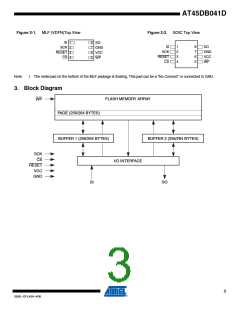
chip select pin (CS) and accessed via a three-wire interface consisting of the Serial Input (SI),
Serial Output (SO), and the Serial Clock (SCK).
All programming and erase cycles are self-timed.
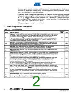
2. Pin Configurations and Pinouts
Table 2-1.
Pin Configurations
Asserted
State
Symbol
Name and Function
Type
Chip Select: Asserting the CS pin selects the device. When the CS pin is deasserted, the device will be deselected
and normally be placed in the standby mode (not Deep Power-Down mode), and the output pin (SO) will be in a
high-impedance state. When the device is deselected, data will not be accepted on the input pin (SI).
CS
Low
Input
A high-to-low transition on the CS pin is required to start an operation, and a low-to-high transition is required to
end an operation. When ending an internally self-timed operation such as a program or erase cycle, the device
will not enter the standby mode until the completion of the operation.
Serial Clock: This pin is used to provide a clock to the device and is used to control the flow of data to and from
the device. Command, address, and input data present on the SI pin is always latched on the rising edge of SCK,
while output data on the SO pin is always clocked out on the falling edge of SCK.
SCK
–
Input
Serial Input: The SI pin is used to shift data into the device. The SI pin is used for all data input including
command and address sequences. Data on the SI pin is always latched on the rising edge of SCK.
SI
–
–
Input
Serial Output: The SO pin is used to shift data out from the device. Data on the SO pin is always clocked out on
the falling edge of SCK.
SO
Output
Write Protect: When the WP pin is asserted, all sectors specified for protection by the Sector Protection Register will
be protected against program and erase operations regardless of whether the Enable Sector Protection command
has been issued or not. The WP pin functions independently of the software controlled protection method. After the
WP pin goes low, the content of the Sector Protection Register cannot be modified.
If a program or erase command is issued to the device while the WP pin is asserted, the device will simply ignore
the command and perform no operation. The device will return to the idle state once the CS pin has been
deasserted. The Enable Sector Protection command and Sector Lockdown command, however, will be
recognized by the device when the WP pin is asserted.
WP
Low
Input
The WP pin is internally pulled-high and may be left floating if hardware controlled protection will not be used.
However, it is recommended that the WP pin also be externally connected to VCC whenever possible.
Reset: A low state on the reset pin (RESET) will terminate the operation in progress and reset the internal state
machine to an idle state. The device will remain in the reset condition as long as a low level is present on the RESET
pin. Normal operation can resume once the RESET pin is brought back to a high level.
RESET
Low
Input
The device incorporates an internal power-on reset circuit, so there are no restrictions on the RESET pin during
power-on sequences. If this pin and feature are not utilized it is recommended that the RESET pin be driven high
externally.
Device Power Supply: The VCC pin is used to supply the source voltage to the device.
VCC
–
–
Power
Operations at invalid VCC voltages may produce spurious results and should not be attempted.
GND
Ground: The ground reference for the power supply. GND should be connected to the system ground.
Ground
2
AT45DB041D
3595L–DFLASH–4/08

 ATMEL [ ATMEL ]