AT90USB82/162
19.9 Registers description
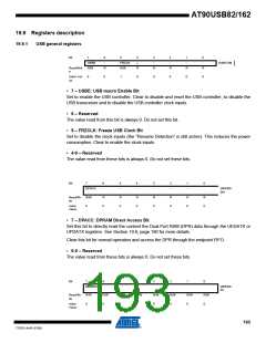
19.9.1
USB general registers
Bit
7
6
-
5
4
-
3
-
2
-
1
-
0
USBE
R/W
FRZLK
R/W
-
USBCON
Read/Writ
e
R
R
R
R
R
R
Initial Val-
ue
0
0
1
0
0
0
0
0
• 7 – USBE: USB macro Enable Bit
Set to enable the USB controller. Clear to disable and reset the USB controller, to disable the
USB transceiver and to disable the USB controller clock inputs.
• 6 – Reserved
The value read from this bit is always 0. Do not set this bit.
• 5 – FRZCLK: Freeze USB Clock Bit
Set to disable the clock inputs (the ”Resume Detection” is still active). This reduces the power
consumption. Clear to enable the clock inputs.
• 4-0 – Reserved
The value read from these bits is always 0. Do not set these bits.
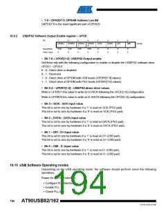
Bit
7
6
5
4
3
2
1
0
DPACC
-
-
-
-
-
-
-
UDPAD-
DH
Read/Wr
ite
R/W
0
R
0
R
0
R
0
R
0
R
0
R
0
R
0
Initial
Value
• 7 – DPACC: DPRAM Direct Access Bit
Set this bit to directly read the content the Dual-Port RAM (DPR) data through the UEDATX or
UPDATX registers. See Section 19.6, page 190 for more details.
Clear this bit for normal operation and access the DPR through the endpoint FIFO.
• 6-0 – Reserved
The value read from these bits is always 0. Do not set these bits.
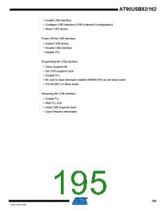
Bit
7
6
5
4
3
2
1
0
DPADD7:0
UDPAD-
DL
Read/Wr
ite
R/W
0
R/W
0
R/W
0
R/W
0
R/W
0
R/W
0
R/W
0
R/W
0
Initial
Value
193
7707D–AVR–07/08

 ATMEL [ ATMEL ]