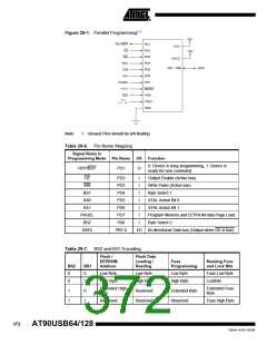
Figure 29-1. Parallel Programming(1)
+5V
+5V
RDY/BSY
OE
PD1
PD2
PD3
PD4
PD5
PD6
PD7
VCC
WR
AVCC
BS1
PB7 - PB0
DATA
XA0
XA1
PAGEL
+12 V
BS2
RESET
PA0
XTAL1
GND
Note:
1. Unused Pins should be left floating.
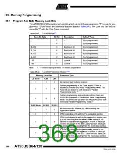
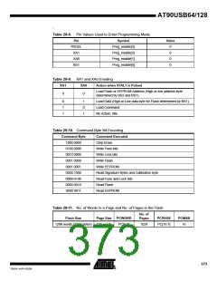
Table 29-6. Pin Name Mapping
Signal Name in
Programming Mode Pin Name
I/O
Function
0: Device is busy programming, 1: Device is
ready for new command.
RDY/BSY
PD1
O
OE
WR
PD2
PD3
PD4
PD5
PD6
PD7
PA0
I
Output Enable (Active low).
Write Pulse (Active low).
Byte Select 1.
I
BS1
I
XA0
I
XTAL Action Bit 0
XA1
I
I
XTAL Action Bit 1
PAGEL
BS2
Program Memory and EEPROM data Page Load.
Byte Select 2.
I
DATA
PB7-0
I/O
Bi-directional Data bus (Output when OE is low).
Table 29-7. BS2 and BS1 Encoding
Flash /
Flash Data
EEPROM
Address
Loading /
Reading
Fuse
Programming
Reading Fuse
and Lock Bits
BS2
0
BS1
0
Low Byte
High Byte
Low Byte
High Byte
Low Byte
High Byte
Fuse Low Byte
Lockbits
0
1
Extended High
Byte
Extended Fuse
Byte
1
1
0
1
Reserved
Reserved
Extended Byte
Reserved
Reserved
Fuse High Byte
372
AT90USB64/128
7593A–AVR–02/06

 ATMEL [ ATMEL ]