control logic is disabled. The USART RX and TX control logic is replaced by a common SPI
transfer control logic. However, the pin control logic and interrupt generation logic is identical in
both modes of operation.
The I/O register locations are the same in both modes. However, some of the functionality of the
control registers changes when using MSPIM.
19.2 Clock Generation
The Clock Generation logic generates the base clock for the Transmitter and Receiver. For
USART MSPIM mode of operation only internal clock generation (i.e. master operation) is sup-
ported. The Data Direction Register for the XCKn pin (DDR_XCKn) must therefore be set to one
(i.e. as output) for the USART in MSPIM to operate correctly. Preferably the DDR_XCKn should
be set up before the USART in MSPIM is enabled (i.e. TXENn and RXENn bit set to one).
The internal clock generation used in MSPIM mode is identical to the USART synchronous mas-
ter mode. The baud rate or UBRRn setting can therefore be calculated using the same
equations, see Table 19-1:
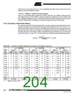
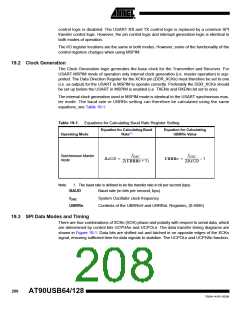
Table 19-1. Equations for Calculating Baud Rate Register Setting
Equation for Calculating Baud
Rate(1)
Equation for Calculating
UBRRn Value
Operating Mode
f
f
Synchronous Master
mode
OSC
OSC
BAUD = --------------------------------------
2(UBRRn + 1)
UBRRn = -------------------- – 1
2BAUD
Note:
1. The baud rate is defined to be the transfer rate in bit per second (bps)
BAUD
Baud rate (in bits per second, bps)
fOSC
System Oscillator clock frequency
UBRRn
Contents of the UBRRnH and UBRRnL Registers, (0-4095)
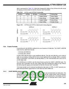
19.3 SPI Data Modes and Timing
There are four combinations of XCKn (SCK) phase and polarity with respect to serial data, which
are determined by control bits UCPHAn and UCPOLn. The data transfer timing diagrams are
shown in Figure 19-1. Data bits are shifted out and latched in on opposite edges of the XCKn
signal, ensuring sufficient time for data signals to stabilize. The UCPOLn and UCPHAn function-
208
AT90USB64/128
7593A–AVR–02/06

 ATMEL [ ATMEL ]