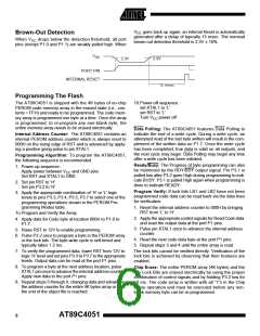
VCC goes back up again, an internal Reset is automatically
generated after a delay of typically 15 msec. The nominal
brown-out detection threshold is 2.3V ± 10%.
Brown-Out Detection
When VCC drops below the detection threshold, all port
pins (except P1.0 and P1.1) are weakly pulled high. When
VCC
2.3V
2.3V
PORT PIN
INTERNAL RESET
15 msec.
Programming The Flash
The AT89C4051 is shipped with the 4K bytes of on-chip
PEROM code memory array in the erased state (i.e., con-
tents = FFH) and ready to be programmed. The code mem-
ory array is programmed one byte at a time. Once the array
is programmed, to re-program any non-blank byte, the
entire memory array needs to be erased electrically.
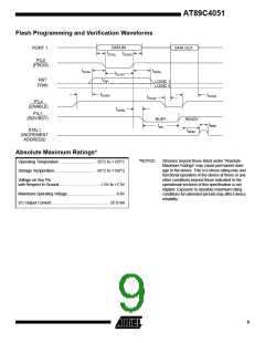
10.Power-off sequence:
set XTAL1 to ’L’
set RST to ’L’
Turn VCC power off
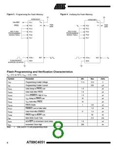
Data Polling: The AT89C4051 features Data Polling to
indicate the end of a write cycle. During a write cycle, an
attempted read of the last byte written will result in the com-
plement of the written data on P1.7. Once the write cycle
has been completed, true data is valid on all outputs, and
the next cycle may begin. Data Polling may begin any time
after a write cycle has been initiated.
Internal Address Counter: The AT89C4051 contains an
internal PEROM address counter which is always reset to
000H on the rising edge of RST and is advanced by apply-
ing a positive going pulse to pin XTAL1.
Programming Algorithm: To program the AT89C4051,
the following sequence is recommended.
Ready/Busy: The Progress of byte programming can also
be monitored by the RDY/BSY output signal. Pin P3.1 is
pulled low after P3.2 goes High during programming to indi-
cate BUSY. P3.1 is pulled High again when programming is
done to indicate READY.
1. Power-up sequence:
Apply power between VCC and GND pins
Set RST and XTAL1 to GND
2. Set pin RST to ’H’
Set pin P3.2 to ’H’
Program Verify: If lock bits LB1 and LB2 have not been
programmed code data can be read back via the data lines
for verification:
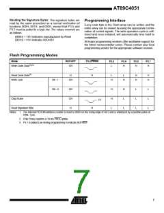
3. Apply the appropriate combination of ’H’ or ’L’ logic
levels to pins P3.3, P3.4, P3.5, P3.7 to select one of the
programming operations shown in the PEROM Pro-
gramming Modes table.
1. Reset the internal address counter to 000H by bringing
RST from ’L’ to ’H’.
To Program and Verify the Array:
2. Apply the appropriate control signals for Read Code data
and read the output data at the port P1 pins.
4. Apply data for Code byte at location 000H to P1.0 to
P1.7.
3. Pulse pin XTAL1 once to advance the internal address
counter.
5. Raise RST to 12V to enable programming.
6. Pulse P3.2 once to program a byte in the PEROM array
or the lock bits. The byte-write cycle is self-timed and
typically takes 1.2 ms.
4. Read the next code data byte at the port P1 pins.
5. Repeat steps 3 and 4 until the entire array is read.
7. To verify the programmed data, lower RST from 12V to
logic ’H’ level and set pins P3.3 to P3.7 to the appropriate
levels. Output data can be read at the port P1 pins.
The lock bits cannot be verified directly. Verification of the
lock bits is achieved by observing that their features are
enabled.
8. To program a byte at the next address location, pulse
XTAL1 pin once to advance the internal address counter.
Apply new data to the port P1 pins.
Chip Erase: The entire PEROM array (4K bytes) and the
two Lock Bits are erased electrically by using the proper
combination of control signals and by holding P3.2 low for
10 ms. The code array is written with all “1”s in the Chip
Erase operation and must be executed before any non-
blank memory byte can be re-programmed.
9. Repeat steps 5 through 8, changing data and advancing
the address counter for the entire 4K bytes array or until
the end of the object file is reached.
AT89C4051
6

 ATMEL [ ATMEL ]