AT89C4051
Restrictions on Certain Instructions
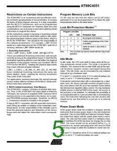
Program Memory Lock Bits
On the chip are two lock bits which can be left unpro-
grammed (U) or can be programmed (P) to obtain the addi-
tional features listed in the table below:
The AT89C4051 is an economical and cost-effective mem-
ber of Atmel’s growing family of microcontrollers. It contains
4K bytes of flash program memory. It is fully compatible
with the MCS-51 architecture, and can be programmed
using the MCS-51 instruction set. However, there are a few
considerations one must keep in mind when utilizing certain
instructions to program this device.
(1)
Lock Bit Protection Modes
Program Lock Bits
All the instructions related to jumping or branching should
be restricted such that the destination address falls within
the physical program memory space of the device, which is
4K for the AT89C4051. This should be the responsibility of
the software programmer. For example, LJMP 0FE0H
would be a valid instruction for the AT89C4051 (with 4K of
memory), whereas LJMP 1000H would not.
LB1
U
LB2
U
Protection Type
1
2
No program lock features.
P
U
Further programming of the Flash
is disabled.
3
P
P
Same as mode 2, also verify is
disabled.
1. Branching instructions:
LCALL, LJMP, ACALL, AJMP, SJMP, JMP @A+DPTR
Note:
1. The Lock Bits can only be erased with the Chip Erase
operation.
These unconditional branching instructions will execute
correctly as long as the programmer keeps in mind that the
destination branching address must fall within the physical
boundaries of the program memory size (locations 00H to
FFFH for the 89C4051). Violating the physical space limits
may cause unknown program behavior.
Idle Mode
In idle mode, the CPU puts itself to sleep while all the on-
chip peripherals remain active. The mode is invoked by
software. The content of the on-chip RAM and all the spe-
cial functions registers remain unchanged during this
mode. The idle mode can be terminated by any enabled
interrupt or by a hardware reset.
CJNE [...], DJNZ [...], JB, JNB, JC, JNC, JBC, JZ, JNZ With
these conditional branching instructions the same rule
above applies. Again, violating the memory boundaries
may cause erratic execution.
P1.0 and P1.1 should be set to ’0’ if no external pullups are
used, or set to ’1’ if external pullups are used.
For applications involving interrupts the normal interrupt
service routine address locations of the 80C51 family archi-
tecture have been preserved.
It should be noted that when idle is terminated by a hard-
ware reset, the device normally resumes program execu-
tion, from where it left off, up to two machine cycles before
the internal reset algorithm takes control. On-chip hardware
inhibits access to internal RAM in this event, but access to
the port pins is not inhibited. To eliminate the possibility of
an unexpected write to a port pin when Idle is terminated by
reset, the instruction following the one that invokes Idle
should not be one that writes to a port pin or to external
memory.
2. MOVX-related instructions, Data Memory:
The AT89C4051 contains 128 bytes of internal data mem-
ory. Thus, in the AT89C4051 the stack depth is limited to
128 bytes, the amount of available RAM. External DATA
memory access is not supported in this device, nor is exter-
nal PROGRAM memory execution. Therefore, no MOVX
[...] instructions should be included in the program.
A typical 80C51 assembler will still assemble instructions,
even if they are written in violation of the restrictions men-
tioned above. It is the responsibility of the controller user to
know the physical features and limitations of the device
being used and adjust the instructions used correspond-
ingly.
Power Down Mode
In the power down mode the oscillator is stopped, and the
instruction that invokes power down is the last instruction
executed. The on-chip RAM and Special Function Regis-
ters retain their values until the power down mode is termi-
nated. The only exit from power down is a hardware reset.
Reset redefines the SFRs but does not change the on-chip
RAM. The reset should not be activated before VCC is
restored to its normal operating level and must be held
active long enough to allow the oscillator to restart and sta-
bilize.
P1.0 and P1.1 should be set to ’0’ if no external pullups are
used, or set to ’1’ if external pullups are used.
5

 ATMEL [ ATMEL ]