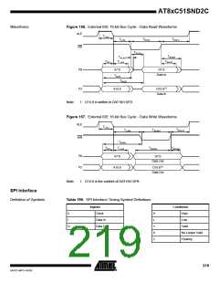
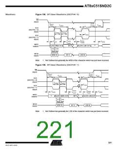
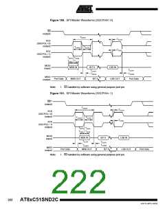
AT8xC51SND2C
Two-wire Interface
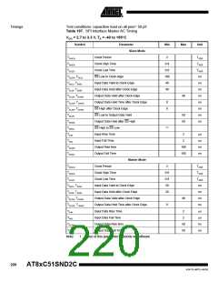
Timings
Table 198. TWI Interface AC Timing
DD = 2.7 to 3.3 V, TA = -40 to +85°C
V
INPUT
Min
OUTPUT
Min
Symbol
THD; STA
TLOW
Parameter
Max
Max
4.0 µs(1)
4.7 µs(1)
4.0 µs(1)
(4)
Start condition hold time
SCL low time
14·TCLCL
16·TCLCL
14·TCLCL
1 µs
(4)
(4)
THIGH
SCL high time
(2)
TRC
SCL rise time
-
TFC
SCL fall time
0.3 µs
0.3 µs(3)
20·TCLCL(4)- TRD
1 µs(1)
TSU; DAT1
TSU; DAT2
TSU; DAT3
THD; DAT
TSU; STA
TSU; STO
TBUF
Data set-up time
250 ns
250 ns
250 ns
0 ns
SDA set-up time (before repeated START condition)
SDA set-up time (before STOP condition)
Data hold time
(4)
8·TCLCL
8·TCLCL(4) - TFC
4.7 µs(1)
(4)
Repeated START set-up time
STOP condition set-up time
Bus free time
14·TCLCL
14·TCLCL
14·TCLCL
1 µs
4.0 µs(1)
(4)
(4)
4.7 µs(1)
(2)
TRD
SDA rise time
-
TFD
SDA fall time
0.3 µs
0.3 µs(3)
Notes: 1. At 100 kbit/s. At other bit-rates this value is inversely proportional to the bit-rate of
100 kbit/s.
2. Determined by the external bus-line capacitance and the external bus-line pull-up
resistor, this must be < 1 µs.
3. Spikes on the SDA and SCL lines with a duration of less than 3·TCLCL will be filtered
out. Maximum capacitance on bus-lines SDA and
SCL= 400 pF.
4. TCLCL= TOSC= one oscillator clock period.
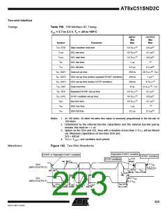
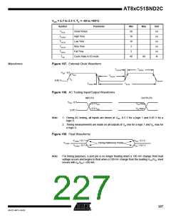
Waveforms
Figure 162. Two Wire Waveforms
Repeated START condition
START or Repeated START condition
Trd
START condition
Tsu;STA
STOP condition
0.7 VDD
0.3 VDD
SDA
(INPUT/OUTPUT)
Tsu;STO
Tbuf
Tfd
Tsu;DAT3
Trc
Tfc
0.7 VDD
0.3 VDD
SCL
(INPUT/OUTPUT)
Thigh
Tsu;DAT2
Tlow
Thd;STA
Thd;DAT
Tsu;DAT1
223
4341D–MP3–04/05

 ATMEL [ ATMEL ]