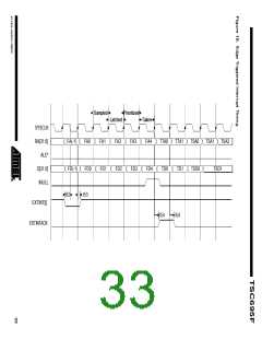
1 (RAM fet2ch()RAM fetch)
3 (DMA session)
(0 cycle min) nth DMA store (0 ws)
4 (RAM fet5ch()RAM fetch)
(null cycle)lead-in (0 cycle min) 1st DMA load (0 ws)
lead-out
cont’
t2
SYSCLK
ALE*
t14
t14
t14
t33
t14
t33
D SAn
t4_1
FA2
t4_1
FA2
t4_1
t32
t32
t21
FA1
FS1
FZ1
D LA1
FA3
FS3
FZ3
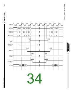
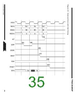
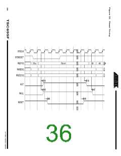
RA[31-0]
RASI[3-0]
(held to the end of RAM access)
(held to the end of RAM access)
t22
t22
t21
D LS1
t4_1
FS2
t4_1
t4_1
t4_1
D SSn
FS2
t4_1
t22
t22
t4_1
FZ2
t21
1 0
t21
1 0
(only word access)
FZ2
RSIZE[1-0]
DMAREQ*
DMAGNT*
DMAAS
(only word access)
t30
t30
early time for DMAREQ* desassertion
t31
t31
t28
t32
t32
t29
t28
t32
t32
t29
t33
t33
t33
t33
t31
t31
t31
t31
RD
(pull-up on WE*)
t5
WRT
MEMCS*[9-0]
DRDY*
t5
t5
t5
t5
t17
t56
t17
t17
t17
t8
t8
t56
OE*
t7
t7
MEMWR*
DDIR
corrected data if needed
t10
t6
t6
t10
t9
t10
t9
t11
t12
t9
(held to the end of RAM access)
t13 t13
t10
t9
t9
t9
FD1
D LD1
D LD1
D SDn
FD2
D[31-0]
DPAR
(from RAM)
(from TSC695F)
t10
t9
FP1
t10
t10
t9
t11
t12
D LP1
(from TSC695F)
D LP1
(from RAM)
t10
DSPn
FP2
Parity generated by TSC695F if dpe =1,
else, same timing as D[31-0]
t10
t9
FC1
t10
corrected parity if needed
t9
t13
D SCn
t13
D LC1
FC2
CB[7-0]
(from RAM)
t16
t16
MHOLD*

 ATMEL [ ATMEL ]