AX88179
USB 3.0 to 10/100/1000M Gigabit Ethernet Controller
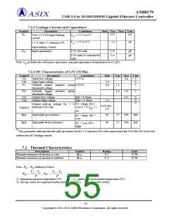
7.1.3 Leakage Current and Capacitance
Symbol
Parameter
Conditions
Min Typ Max Unit
IIN
-
≤±1
-
μA
True 3.3 V I/O input leakage
current
Vin = 3.3 V or 0 V
Vin = 5 V or 0 V
-
<±1
-
pF
3.3 V with 5 V tolerance I/O
Input leakage current
Input capacitance
CIN
3.3V I/O cells
-
-
2.25
3.6
-
-
pF
pF
3.3V with 5V tolerant I/O
cells
Note: CIN includes the cell layout capacitance and pad capacitance (Estimated to be 0.5 pF).
7.1.4 DC Characteristics of 3.3V I/O Pins
Symbol
Vil
Vih
Parameter
Input low voltage
Input high voltage
Schmitt trigger negative going LVTTL
threshold voltage
Conditions
LVTTL
Min
-
2.0
0.8
Typ Max Unit
-
-
0.8
-
-
V
V
V
Vt-
1.1
Vt+
Schmitt trigger positive going
threshold voltage
-
1.6
2.0
V
Vol
Voh
Output low voltage
Output high voltage
|Iol| = 4~8mA
|Ioh| = 4~8mA
-
2.4
-
-
0.4
-
V
V
V
Output pull-up voltage for 5 V PU = High, PD =
tolerance I/O cells
VCC3IO –
Low E = 0, |Ipu| = 1
Vopu[1]
Rpu
-
-
0.9
μA
Input pull-up resistance
Input pull-down resistance
40
40
75
190
KΩ
KΩ
PU = High, PD =
Low
Rpd
75
190
PU = Low, PD =
High
[1] This parameter indicates that the pull-up resistor for the 5 V tolerance I/O cells cannot reach the VCC3IO DC level even
without the DC loading current.
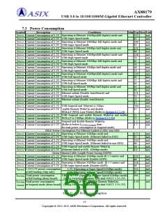
7.2 Thermal Characteristics
Description
Symbol
Θ JC
Rating
8.3
Units
°C/W
Thermal resistance of junction to case
Thermal resistance of junction to ambient
21.4
°C/W
Θ JA
Note: JA
, JC defined as below
TJ TA
TJ TC
JA
=
,
JC
=
P
P
TJ: maximum junction temperature (°C)
TA: ambient or environment temperature (°C)
TC: the top center of compound surface temperature (°C) P: input power (watts)
54
Copyright © 2011-2012 ASIX Electronics Corporation. All rights reserved.

 ASIX [ ASIX ELECTRONICS CORPORATION ]