DS1600SPE Data Sheet
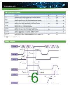
Control and Status Signals
Output Signals
PS_PRESENT
Signal used to indicate to the system that a power supply is inserted in the power bay. This pin is shorted to the standby return in the power supply. Recommended
pull-up resistor to 12 VSB is 8.2 k with a 3.0 k pull-down to ground. A 100 pF decoupling capacitor is also recommended.
PS_INTERRUPT
Active low signal used by the power supply to indicate to the system that a change in power supply status has occurred. This event can be triggered by faults such
as OVP, OCP, OTP, and fan fault. This signal can be cleared by a CLEAR_FAULT command. Recommended pull-up resistor to 12 VSB is 8.2 k with a 3.0 k
pull-down to ground. A 100 pF decoupling capacitor is also recommended.
MIN
MAX
0.8 V
5.0 V
4 mA
4 mA
VIL
Output logic level LOW
VIH
Output logic level HIGH
2.0 V
ISOURCE
ISINK
Current that may be sourced by this pin
Current that may be sunk by this pin at low state
BUS Signals
ISHARE
Bus signal used by the power supply for active current sharing. All power supplies configured in the system for n+n sharing will refer to this bus voltage inorder to
load share.
Voltage Range
The range of this signal for active sharing will be up to 8.0 V, which corresponds to the maximum output current.
MIN
7.75
3.85
MAX
ISHARE Voltage
Voltage at 100% load, stand-alone unit
Voltage at 50% load, stand-alone unit
Current that may be sourced by this pin
8.25
4.15
ISOURCE
160 mA
SCL, SDA, A0, A1, A2
Clock, data and addressing signals defined as per I2C requirements. It is recommended that these pins be pulled-up to a 2.2 kohm resistor to 3.3 V and a 22 pF
decoupling capacitor at the system side.
MIN
MAX
0.8 V
5.0 V
VL
Logic level LOW
Logic level HIGH
VH
2.0 V
Note: All signal noise levels are below 400 mVpk-pk from 0 - 100 MHz.
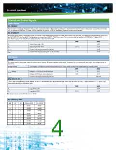
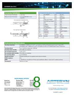
I2C Addressing Table
A2
0
A1
0
A0
0
PMBus (W/R)
B0/B1
FRU (W/R)
A0/A1
A2/A3
A4/A5
A6/A7
A8/A9
AA/AB
AC/AD
AE/AF
0
0
1
B2/B3
0
1
0
B4/B5
0
1
1
B6/B7
1
0
0
B8/B9
1
0
1
BA/BB
BC/BD
BE/BF
1
1
0
1
1
1

 ARTESYN [ ARTESYN TECHNOLOGIES ]