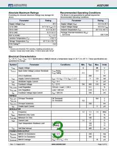
AOZ1280
Detailed Description
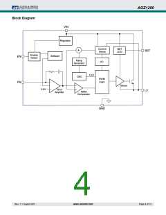
The AOZ1280 is a current-mode step down regulator
with integrated high side NMOS switch. It operates from
a 3 V to 26 V input voltage range and supplies up to 1.2 A
of load current. Features include: enable control, under
voltage lock-out, internal soft-start, output over-voltage
protection, over-current protection, and thermal shut
down.
Switching Frequency
The AOZ1280 switching frequency is fixed and set by an
internal oscillator. The switching frequency is set
internally 1.5 MHz.
Output Voltage Programming
Output voltage can be set by feeding back the output to
the FB pin with a resistor divider network. In the
application circuit shown in Figure 1. The resistor divider
network includes R1 and R2. Usually, a design is started
by picking a fixed R2 value and calculating the required
R1 with equation below.
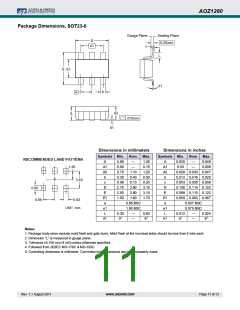
The AOZ1280 is available in SOT23-6L package.
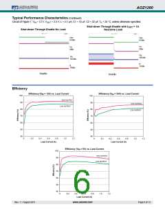
Enable and Soft Start
The AOZ1280 has an internal soft start feature to limit
in-rush current and ensure the output voltage ramps up
smoothly to regulation voltage. A soft start process
begins when the input voltage rises to a voltage higher
than UVLO and the voltage level on the EN pin is HIGH.
In the soft start process, the output voltage is typically
ramped to regulation voltage in 400 s. The 400 s
soft start time is set internally.
R
1
------
V
= 0.8 1 +
O
R
2
Some standard values of R1 and R2 for the most
commonly used output voltage values are listed in
Table 1.
The EN pin of the AOZ1280 is active high. Connect the
EN pin to VIN if the enable function is not used. Pulling
EN to ground will disable the AOZ1280. Do not leave EN
open. The voltage on the EN pin must be above 1.2 V to
enable the AOZ1280. When voltage on the EN pin falls
below 0.4 V, the AOZ1280 is disabled.
Table 1.
Vo (V)
R1 (kΩ)
R2 (kΩ)
1.8
2.5
3.3
5.0
80.6
49.9
49.9
49.9
64.2
23.4
15.8
9.53
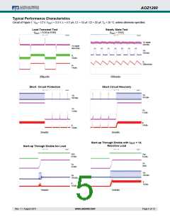
Steady-State Operation
Under steady-state conditions, the converter operates
in fixed frequency and Continuous-Conduction Mode
(CCM).
The combination of R1 and R2 should be large enough to
avoid drawing excessive current from the output, which
will cause power loss.
The AOZ1280 integrates an internal NMOS as the
high-side switch. Inductor current is sensed by amplifying
the voltage drop across the drain to the source of the
high-side power MOSFET. Output voltage is divided
down by the external voltage divider at the FB pin.
The difference of the FB pin voltage and reference
voltage is amplified by the internal transconductance
error amplifier. The error voltage is compared against the
current signal, which is sum of inductor current signal
plus ramp compensation signal, at the PWM comparator
input. If the current signal is less than the error voltage,
the internal high-side switch is on. The inductor current
flows from the input through the inductor to the output.
When the current signal exceeds the error voltage, the
high-side switch is off. The inductor current is
Protection Features
The AOZ1280 has multiple protection features to prevent
system circuit damage under abnormal conditions.
Over Current Protection (OCP)
The sensed inductor current signal is also used for over
current protection.
The cycle-by-cycle current limit threshold is set normal
value of 2 A. When the load current reaches the current
limit threshold, the cycle-by-cycle current limit circuit
immediately turns off the high-side switch to terminate
the current duty cycle. The inductor current stop rising.
The cycle-by-cycle current limit protection directly limits
inductor peak current. The average inductor current is
also limited due to the limitation on peak inductor current.
When cycle-by-cycle current limit circuit is triggered, the
output voltage drops as the duty cycle decreasing.
freewheeling through the external Schottky diode to
output.
Rev. 1.1 August 2011
www.aosmd.com
Page 7 of 13

 AOS [ ALPHA & OMEGA SEMICONDUCTORS ]