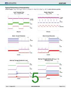
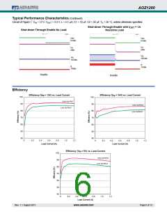
AOZ1280
The power dissipation in Schottky can be approximated
as:
Several layout tips are listed below for the best electric
and thermal performance.
P
= I 1 – D V
O FW_Schottky
1. The input capacitor should be connected as close as
possible to the VIN pin and the GND pin.
diode_loss
2. The inductor should be placed as close as possible
to the LX pin and the output capacitor.
where,
VFW_Schottky is the Schottky diode forward voltage drop.
3. Keep the connection of the schottky diode between
the LX pin and the GND pin as short and wide
as possible.
The power dissipation of inductor can be approximately
calculated by output current and DCR of inductor.
2
P
= I R
1.1
inductor
4. Place the feedback resistors and compensation
components as close to the chip as possible.
inductor_loss
O
5. Keep sensitive signal traces away from the LX pin.
The actual junction temperature can be calculated with
power dissipation in the AOZ1280 and thermal
impedance from junction to ambient.
6. Pour a maximized copper area to the VIN pin, the
LX pin and especially the GND pin to help thermal
dissipation.
T
junction
7. Pour a copper plane on all unused board area and
connect the plane to stable DC nodes, like VIN,
GND or VOUT.
= P
–P
+ T
inductor_loss amb
JA
total_loss
The maximum junction temperature of AOZ1280 is
150 ºC, which limits the maximum load current capability.
The thermal performance of the AOZ1280 is strongly
affected by the PCB layout. Extra care should be taken
by users during design process to ensure that the IC will
operate under the recommended environmental
conditions.
Rev. 1.1 August 2011
www.aosmd.com
Page 10 of 13

 AOS [ ALPHA & OMEGA SEMICONDUCTORS ]