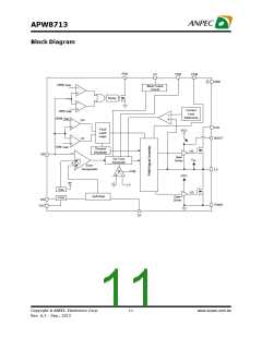
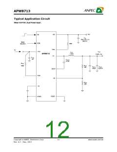
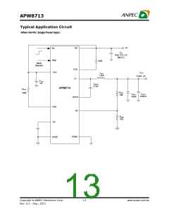
APW8713
Pin Description
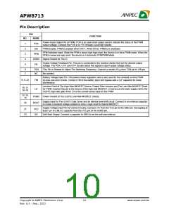
PIN
FUNCTION
NO.
1
NAME
POK
EN
Power-Good Output Pin of PWM. POK is an open-drain output used to indicate the status of the PWM
output voltage. Connect the POK in to +5V through a pull-high resistor.
2
PWM Enable. PWM is enabled when EN=1. When EN=0, PWM is in shutdown.
PFM Selection Input. When the PFM is above high logic level, the Device is in force PWM mode. When the
PFM is below low logic level, the device is in automatic PFM/PWM Mode.
3
PFM
AGND
FB
4
Signal Ground for The IC.
Output Voltage Feedback Pin. This pin is connected to the resistive divider that set the desired output
voltage. The POK, UVP, and OVP circuits detect this signal to report output voltage status.
5
6
7
TON
NC
This Pin is Allowed to Adjust The Switching Frequency. Connect a resistor RTON from TON pin to VIN pin.
No connect.
Battery Voltage Input Pin. VIN powers linear regulators and is also used for the constant on-time PWM
on-time one-shot circuits. Connect VIN to the battery input and bypass with a 1mF capacitor for noise
interference.
8, 9, 22
VIN
LX
Junction Point of The High-Side MOSFET Source, Output Filter Inductor and The Low-Side MOSFET Drain
for PWM. Connect this pin to the Source of the high-side MOSFET. LX serves as the lower supply rail for the
UGATE high-side gate driver. LX is the current-sense input for the PWM.
10, 11,
16~18
12~15,
19
PGND
BOOT
Power Ground of The LGATE Low-Side MOSFET Drivers.
Supply Input for The UGATE Gate Driver and an internal level-shift circuit. Connect to an external capacitor
to create a boosted voltage suitable to drive a logic-level N-channel MOSFET.
20
Supply Voltage Input Pin for Control Circuitry, Connect +5V from the VCC pin to the GND pin. Decoupling at
least 1mF of a MLCC capacitor from the VCC pin to the AGND pin.
21
23
VCC
SS
Soft Start Output. Connect a capacitor to GND to set the soft start interval.
Copyright ã ANPEC Electronics Corp.
10
www.anpec.com.tw
Rev. A.3 - Sep., 2013

 ANPEC [ ANPEC ELECTRONICS COROPRATION ]