APW7302B
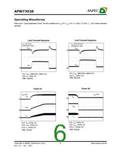
Operating Waveforms
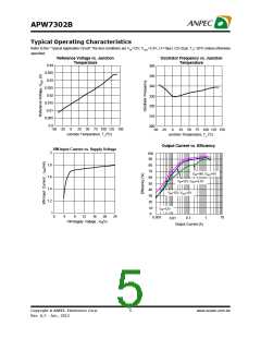
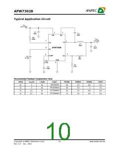
Refer to the “Typical Application Circuit” The test conditions are VIN=12V, VOUT=3.3V, L1=10mH, C2=22mF, TA= 25oC unless otherwise
specified.
Load Transient Response
Load Transient Response
IOUT=0A-2A-0A,
IOUT=0.5A-2A-0.5A,
rise/fall tim e=10ms
rise/falltim e=10ms
VOUT
VOUT
1
1
IOUT
IOUT
2
2
CH1: VOUT, 200mV/Div, offset=3.3V
CH2: IL1, 1A/Div, DC
CH1: VOUT, 200mV/Div, offset=3.3V
CH2: IL1, 1A/Div, DC
TIME: 50ms/Div
TIME: 50ms/Div
Power Off
Power On
IOUT=2A
IOUT=2A
IOUT=5A
VIN
VIN
1
1
VOUT
VOUT
2
3
2
3
IL1
IL1
CH1: VIN, 5V/Div, DC
CH2: VOUT, 2V/Div, DC
CH3: IL1, 2A/Div, DC
CH1: VIN, 5V/Div, DC
CH2: VOUT, 2V/Div, DC
CH3: IL1, 2A/Div, DC
TIME: 5ms/Div
TIME: 5ms/Div
Copyright ã ANPEC Electronics Corp.
6
www.anpec.com.tw
Rev. A.2 - Jan., 2012

 ANPEC [ ANPEC ELECTRONICS COROPRATION ]