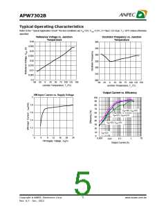
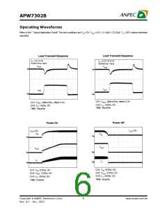
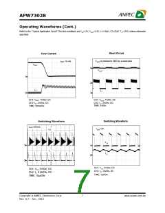
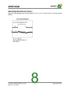
APW7302B
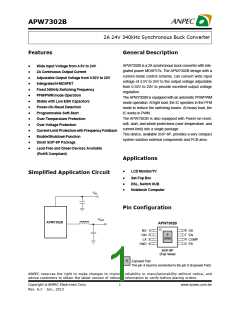
Ordering and Marking Information
Package Code
KA : SOP-8P
APW7302B
Temperature Range
Assembly Material
Handling Code
I : -40 to 85 oC
Handling Code
TR : Tape & Reel
Assembly Material
G : Halogen and Lead Free Device
Temperature Range
Package Code
APW7302B
XXXXX
APW7302B KA:
XXXXX - Date Code
Note: ANPEC lead-free products contain molding compounds/die attach materials and 100% matte tin plate termination finish; which
are fully compliant with RoHS. ANPEC lead-free products meet or exceed the lead-free requirements of IPC/JEDEC J-STD-020D for
MSL classification at lead-free peak reflow temperature. ANPEC defines “Green” to mean lead-free (RoHS compliant) and halogen
free (Br or Cl does not exceed 900ppm by weight in homogeneous material and total of Br and Cl does not exceed 1500ppm by
weight).
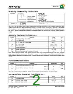
Absolute Maximum Ratings (Note 1)
Symbol
Parameter
Rating
-0.3 ~ 30
Unit
V
VIN
VIN Supply Voltage (VIN to GND)
VLX
LX to GND Voltage
-1 ~VIN+0.3
-0.3 ~ 6
V
EN, FB, COMP, SS to GND Voltage
BS to GND Voltage
V
VBS
PD
VLX-0.3 ~ VLX+6
Internally Limited
150
V
Power Dissipation
W
oC
oC
oC
TJ
Junction Temperature
TSTG
TSDR
Storage Temperature
-65 ~ 150
260
Maximum Lead Soldering Temperature, 10 Seconds
Note1: Stresses beyond those listed under "absolute maximum ratings" may cause permanent damage to the device. These are
stress ratings only and functional operation of the device at these or any other conditions beyond those indicated under "recom-
mended operating conditions" is not implied. Exposure to absolute maximum rating conditions for extended periods may affect device
reliability
Thermal Characteristics
Symbol
Parameter
Typical Value
Unit
Junction-to-Ambient Resistance in Free Air (Note 2)
oC/W
qJA
SOP-8P
SOP-8P
50
10
Junction-to-Case Resistance in Free Air
oC/W
qJC
Note 2: qJA is measured with the component mounted on a high effective thermal conductivity test board in free air.
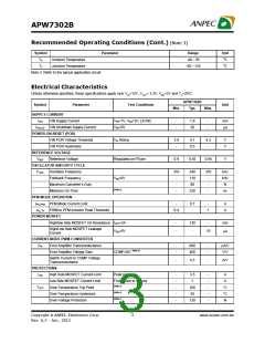
Recommended Operating Conditions (Note 3)
Symbol
Parameter
Range
4.5 ~ 24
0.92 ~ 20
0 ~ 2
Unit
V
VIN
VIN Supply Voltage
VOUT
IOUT
Converter Output Voltage
Converter Output Current
V
A
Copyright ã ANPEC Electronics Corp.
2
www.anpec.com.tw
Rev. A.2 - Jan., 2012

 ANPEC [ ANPEC ELECTRONICS COROPRATION ]