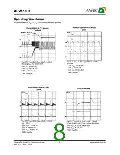
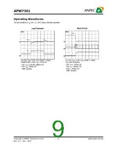
APW7301
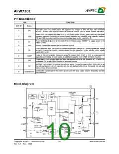
Function Description
Main Control Loop
Enable/Shutdown
The APW7301 is a constant frequency current mode
switching regulator. During normal operation, the inter-
nal N-channel power MOSFET is turned on each cycle
when the oscillator sets an internal RS latch and would
be turned off when an internal current comparator (ICMP)
resets the latch. The peak inductor current at which ICMP
resets the RS latch is controlled by the voltage on the
COMP pin, which is the output of the error amplifier
(EAMP). An external resistive divider connected between
VOUT and ground allows the EAMP to receive an output
feedback voltage VFB at FB pin. When the load current
increases, it causes a slight decrease in VFB relative to
the 0.925V reference, which in turn causes the COMP
voltage to increase until the average inductor current
matches the new load current.
Driving EN to ground places the APW7301 in shutdown.
When in shutdown, the internalN-Channel power MOSFET
turns off, all internal circuitry shuts down and the quies-
cent supply current reduces to 0.3mA.
Current-Limit Protection
The APW7301 monitors the output current, flowing
through the N-Channel power MOSFET, and limits the
IC from damages during overload, short-circuit and over-
voltage conditions.
FrequencyFoldback
The foldback frequency is controlled by the FB voltage.
When the FB pin voltage is under 0.6V, the frequency of
the oscillator will be reduced to 110kHz. This lower fre-
quency allows the inductor current to safely discharge,
thereby preventing current runaway. The oscillator’s fre-
quency will switch to its designed rate when the feedback
voltage on FB rises above the rising frequency foldback
threshold (0.6V, typical) again.
VIN Power-On-Reset (POR) and EN Under-voltage
Lockout
The APW7301 keep monitoring the voltage on VIN pin to
prevent wrong logic operations which may occur when
VIN voltage is not high enough for the internal control
circuitry to operate. The VIN POR has a rising threshold
of 4.05V (typical) with 0.3V of hysteresis.
Over-Voltage Protection
An external under-voltage lockout (UVLO) is sensed at
the EN pin. The EN UVLO has a rising threshold of 2.5V
with 0.2V of hysteresis. The EN pin should be connected
a resistor divider from VIN to EN .
The over-voltage function monitors the output voltage by
FB pin. When the FB voltage increase over 120% of the
reference voltage, the over-voltage protection compara-
tor will force the high-and low-side MOSFET gate driver
off. As soon as the output voltage is within regulation, the
OVP comparator is disengaged. The chip will restore its
normal operation.
After the VIN and EN voltages exceed their respective
voltage thresholds, the IC starts a start-up process and
then ramps up the output voltage to the setting of output
voltage.
Over-Temperature Protection (OTP)
The over-temperature circuit limits the junction tempera-
ture of the APW7301 When the junction temperature ex-
ceeds TJ =+160oC, a thermal sensor turns off the power
MOSFET, allowing the device to cool down. The thermal
sensor allows the converter to start a start-up process
and regulate the output voltage again after the junction
temperature cools by 50oC.
The OTP designed with a 50oC hysteresis lowers the
average TJ during continuous thermal overload
conditions, increasing life time of the IC.
Copyright ã ANPEC Electronics Corp.
12
www.anpec.com.tw
Rev. A.2 - Apr., 2013

 ANPEC [ ANPEC ELECTRONICS COROPRATION ]