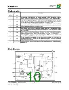
APW7301
Pin Description
PIN
FUNCTION
SOP-8P
Name
High-Side Gate Drive Boost Input. BS supplies the voltage to drive the high-side N-channel
MOSFET. At least 10nF capacitor should be connected from LX to BS to supply the high side switch.
1
BS
Power Input. VIN supplies the power (4.5V to 24V) to the control circuitry, gate drivers and step-down
converter switches. Connecting a ceramic bypass capacitor and a suitably large capacitor between
VIN and GND eliminates switching noise and voltage ripple on the input to the IC.
2
VIN
Power Switching Output. LX is the Drain of the N-Channel power MOSFET to supply power to the
output LC filter.
3
4
LX
GND
Ground. Connect the exposed pad on backside to Pin 4.
Output feedback Input. The APW7301 senses the feedback voltage via FB and regulates the voltage
at 0.925V. Connecting FB with a resistor-divider from the converter’s output sets the output voltage
from 0.925V to 20V.
5
FB
Output of the error amplifier. Connect a series RC network from COMP to GND to compensate the
regulation control loop. In some cases, an additional capacitor from COMP to GND is required.
6
7
COMP
EN
Enable Input. EN is a digital input that turns the regulator on or off. EN threshold is 2.5V with 0.2V
hysteresis. Pull up with 100kW resistor for automatic startup.
Soft-Start Control Input. SS controls the soft-start period. Connect a capacitor from SS to GND to set
the soft-start period. A 0.1mF capacitor sets the soft-start period to 15ms. To disable the soft-start
feature, leave SS unconnected.
8
9
SS
Connect the exposed pad to the system ground plan with large copper area for dissipating heat into
the ambient air.
Exposed Pad
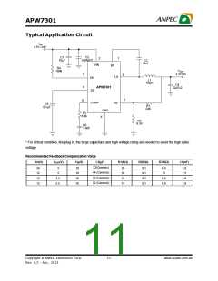
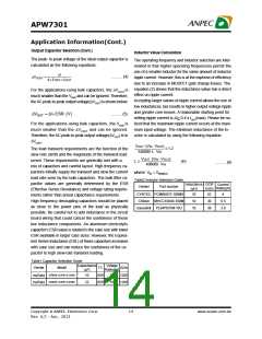
Block Diagram
VIN
2
Current Sense
Amplifier
LOC
Over
Temperature
Protection
Power-On-
Reset
Current
Limit
5V
1
BS
POR
5V
OTP
120%VREF
6mA
Gate
Driver
Fault
Logics
SS 8
OVP
Inhibit
Gate
Control
3
4
LX
5V
5
FB
Gm
Current
Compartor
Error
VREF
Gate
Driver
Amplifier
GND
COMP 6
2.5/2.3V
UVLO
Slope
Compensation
LOC
Oscillator
340kHz/
110kHz
Current Sense
Amplifier
Enable
VIN
7
EN
5V
Internal
Regulator
FB
1.5V
0.6V
Copyright ã ANPEC Electronics Corp.
10
www.anpec.com.tw
Rev. A.2 - Apr., 2013

 ANPEC [ ANPEC ELECTRONICS COROPRATION ]