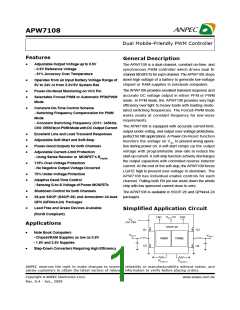
APW7108
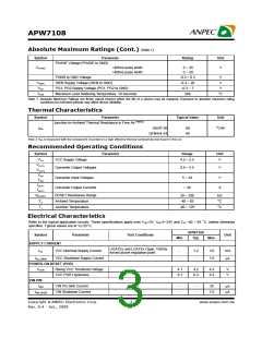
Absolute Maximum Ratings (Cont.) (Note 1)
Symbol
Parameter
Rating
Unit
PHASE Voltage (PHASE to GND)
VPHASE
<400ns pulse width
>400ns pulse width
-5 ~ 35
-2 ~ 28
V
PGND to GND Voltage
-0.3 ~ 0.3
-0.3 ~ 28
-0.3 ~ 7
260
V
V
VISEN
VPG
ISEN Supply Voltage (ISEN to GND)
PG1, PG2 Supply Voltage (PG1, PG2 to GND)
V
oC
TSDR
Maximum Lead Soldering Temperature, 10 Seconds
Note 1: Absolute Maximum Ratings are those values beyond which the life of a device may be impaired. Exposure to absolute maximum rating
conditions for extended periods may affect device reliability.
Thermal Characteristics
Symbol
Parameter
Typical Value
Unit
Junction-to-Ambient Thermal Resistance in Free Air (Note 2)
SSOP-28
80
40
oC/W
qJA
QFN4x4-24
Note 2: qJA is measured with the component mounted on a high effective thermal conductivity test board in free air.
Recommended Operating Conditions
Symbol
Parameter
Range
Unit
VCC
VCC Supply Voltage
4.5 ~ 5.5
V
VOUT1
VOUT2
VIN1
Converter Output Voltages
0.9 ~ 5.5
5 ~ 24
~ 20
V
V
A
Converter Input Voltages
Converter Output Currents
VIN2
IOUT1
IOUT2
ROCSET
TA
OCSET Resistance Range
Ambient Temperature
Junction Temperature
39 ~ 200
-40 ~ 85
-40 ~ 125
kW
oC
oC
TJ
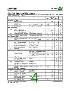
Electrical Characteristics
Refer to the typical application circuits. These specifications apply over VCC=5V, VIN=5~24V and TA= -40 ~ 85 °C, unless otherwise
specified. Typical values are at TA=25°C.
APW7108
Symbol
Parameter
Test Conditions
Unit
Min.
Typ.
Max.
SUPPLY CURRENT
UGATEx and LGATEx Open, VSENx
forced above regulation point
ICC
VCC Nominal Supply Current
VCC Shutdown Supply Current
-
-
1.2
-
3.0
1.0
mA
ICC_SHDN
mA
POWER-ON-RESET (POR)
VCCR Rising VCC Threshold Voltage
4.1
0.1
4.2
0.2
4.3
0.3
V
V
VCC POR Hysteresis
VIN PIN
VIN Pin Sink Current
VIN Shutdown Current
-
-
-
-
35
IVIN
mA
mA
1.0
IVIN_SHDN
Copyright ã ANPEC Electronics Corp.
3
www.anpec.com.tw
Rev. A.4 - Jan., 2009

 ANPEC [ ANPEC ELECTRONICS COROPRATION ]