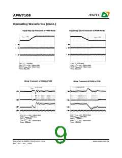
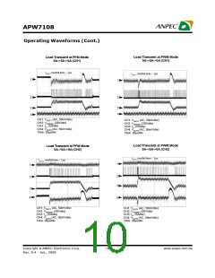
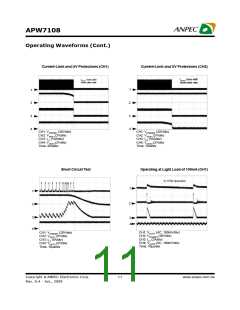
APW7108
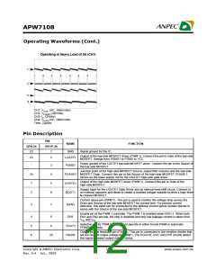
Pin Description (Cont.)
PIN
NAME
FUNCTION
QFN-24
SSOP-28
Current-limit threshold setting pin (PWM1). This pin is a buffered 0.9V internal reference
OCSET1 voltage. A resistor from this pin to the ground sets the current limit threshold for the
converter.
-
11
Soft-start and soft-stop interval setting pin. The SOFT1 pin can source 4.5µA in soft-start
process or sink 2.2mA in soft-stop process. The SOFT1 current charges or discharges
the capacitor connected from the pin to the GND. The output voltage of the converter
follows the ramping-up/down voltage on the SOFT1 pin in the soft-start/soft-stop process
with the SOFT1 pin voltage as reference. When the SOFT1 pin voltage is higher than
internal reference 0.9V, the error amplifier will use the reference to regulate output
voltage. In the event of under-voltage, or EN1 shutdown, the SOFT1 is used by the
soft-stop function and then pulled down though a 2K resistor to the ground after the
falling SOFT1 voltage reaches about 50mV threshold. In soft-stop process, the converter
only has sinking capability even though the output voltage is below the regulated
voltage.
8
12
SOFT1
-
13
14
NC
No comment
9
VIN
Battery voltage input pin.
Power-good output pin of PWM 1. PGOOD1 is an open drain output used to indicate the
status of the output voltage. This pin is pulled low when the PWM 1 Converter output is
out of -11% ~ +15% of the set value.
10
15
PG1
11
12
16
17
PG2
Power-good output pin of PWM 2. The function is same as the PG1 pin.
SOFT2
Soft-start and soft-stop interval setting pin. The function is the same as the SOFT1 pin.
Current-limit threshold setting pin (PWM 2). This pin is a buffered 0.9V internal reference
-
18
OCSET2 voltage. A resistor from this pin to ground sets the current-limit threshold for the
converter.
Output voltage feedback pin. This pin is connected to the resistive divider that set the
13
14
15
19
20
21
VSEN2
VOUT2
EN2
desired output voltage for PWM 2. The PGOOD, UVP, and OVP circuits use this signal to
report output voltage status.
Selection pin for PWM 2 controller to operate in either forced PWM or automatic
PFM/PWM mode.
Enable pin of the PWM 2 controller. The PWM 2 is enabled when EN2 = 1. When both
EN1 and EN2 are low, the chip is disabled and only low leakage current is taken from
VCC and VIN.
16
17
22
23
ISEN2
Current sense pin (PWM 2). This pin has the same function as ISEN1.
Supply Input for the UGATE2 Gate Driver and an internal level-shift circuit. Its function is
same as BOOT1.
BOOT2
Output of the high-side MOSFET driver (PWM 2). Connect this pin to Gate of the
high-side MOSFET.
18
19
-
24
25
26
UGATE2
Junction point of the high-side MOSFET source, output filter inductor and the low-side
PHASE2 MOSFET Drain. Connect this pin to the Source of the high-side MOSFET. PHASE2
serves as the lower supply rail for the UGATE2 high-side gate driver.
Power ground of the LGATE2 low-side MOSFET driver. Connect the pin to the Source of
the low-side MOSFET.
PGND2
Output of the low-side MOSFET driver (PWM 2). Connect this pin to Gate of the low-side
MOSFET. Swings from PGND2 or PGND to VCC.
20
21
27
28
LGATE2
VCC
Supply voltage input pin for control circuitry and both low-side MOSFET drivers.
Current limit threshold setting pin for PWM1 and PWM 2. This pin is a buffered 0.9V
internal reference voltage. A resistor from this pin to the ground sets the current-limit
threshold for the converter.
7
-
-
OCSET
Thermal
Pad
Power ground of the both channels’ low-side MOSFET drivers. Connect the Sources of
the both channels' low-side MOSFETs to the IC thermal pad as close as possible.
PGND
Copyright ã ANPEC Electronics Corp.
13
www.anpec.com.tw
Rev. A.4 - Jan., 2009

 ANPEC [ ANPEC ELECTRONICS COROPRATION ]