APL3512
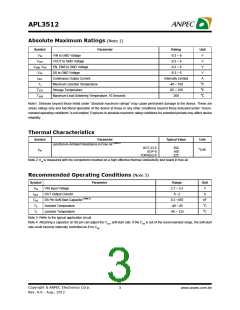
Absolute Maximum Ratings (Note 1)
Symbol
VIN
Parameter
Rating
-0.3 ~ 6
Unit
V
VIN to GND Voltage
VOUT
VENB, VEN
VSS
VOUT to GND Voltage
EN, ENB to GND Voltage
SS to GND Voltage
-0.3 ~ 6
V
-0.3 ~ 6
V
-0.3 ~ 6
V
IOUT
Continuous Output Current
Maximum Junction Temperature
Storage Temperature
Internally Limited
-40 ~ 150
-65 ~ 150
260
A
TJ
oC
oC
oC
TSTG
TSDR
Maximum Lead Soldering Temperature, 10 Seconds
Note1: Stresses beyond those listed under "absolute maximum ratings" may cause permanent damage to the device. These are
stress ratings only and functional operation of the device at these or any other conditions beyond those indicated under "recom-
mended operating conditions" is not implied. Exposure to absolute maximum rating conditions for extended periods may affect device
reliability.
Thermal Characteristics
Symbol
Parameter
Typical Value
Unit
Junction-to-Ambient Resistance in Free Air (Note 2)
SOT-23-5
SOP-8
TDFN2x2-6
250
160
225
oC/W
qJA
Note 2: qJA is measured with the component mounted on a high effective thermal conductivity test board in free air.
Recommended Operating Conditions (Note 3)
Symbol
Parameter
Range
2.7 ~ 5.5
0 ~2
Unit
VIN
VIN Input Voltage
V
A
IOUT
CSS
TA
OUT Output Current
SS Pin Soft-Start Capacitor (Note 4)
Ambient Temperature
Junction Temperature
0.3 ~470
-40 ~ 85
-40 ~ 125
nF
oC
oC
TJ
Note 3: Refer to the typical application circuit.
Note 4: Attaching a capacitor on SS pin can adjust the VOUT soft-start rate. If the CSS is out of the recommended range, the soft-start
rate could become internally controlled as if no CSS.
Copyright ã ANPEC Electronics Corp.
3
www.anpec.com.tw
Rev. A.6 - Aug., 2012

 ANPEC [ ANPEC ELECTRONICS COROPRATION ]