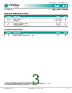
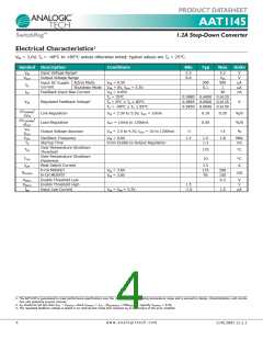
PRODUCT DATASHEET
AAT1145
SwitchRegTM
1.2A Step-Down Converter
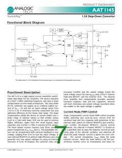
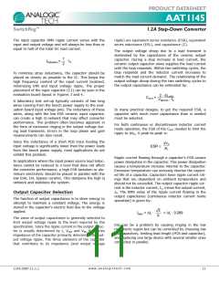
Functional Block Diagram
SLOPE
COMP
OSC
IN
VIN 2.5V to 5.5V
ISENSE
AMP
0.6V
Softstart
SET
RESET
PWM
LOGIC
VOUT
ICOMP
LX
NON-OVERLAP
CONTROL
L1
OUT
R1*
R2*
R1*
COUT
OVDET
0.65V
R2*
Over-Temperature
VIN
and Short-Circuit
IZERO
COMP
Protection
PGND
0.6V
SHUTDOWN
REF
EN
AIN AGND
*The resistor divider R1 + R2 is internally set for the fixed output versions, and is externally set for the adjustable output versions.
increases to100% and the output voltage tracks the
input voltage minus the low RDS(ON) drop of the P-channel
high-side MOSFET and the inductor DCR. The internal
error amplifier and compensation provides excellent
transient response, load and line regulation. Internal
soft start eliminates any output voltage overshoot when
the enable or the input voltage is applied.
Functional Description
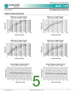
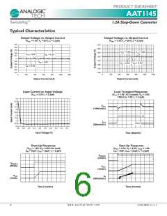
The AAT1145 is a high output current monolithic switch-
mode step-down DC-DC converter. The device operates
at a fixed 1.5MHz switching frequency, and uses a slope
compensated current mode architecture. This step-down
DC-DC converter can supply up to 1200mA output cur-
rent at VIN = 3V and has an input voltage range from
2.5V to 5.5V. It minimizes external component size and
optimizes efficiency at the heavy load range. The slope
compensation allows the device to remain stable over a
wider range of inductor values so that smaller values
(1μH to 4.7μH) with lower DCR can be used to achieve
higher efficiency. Apart from the small bypass input
capacitor, only a small L-C filter is required at the output.
The fixed output version requires only three external
power components (CIN, COUT, and L). The adjustable ver-
sion can be programmed with external feedback to any
voltage, ranging from 0.6V to near the input voltage. It
uses internal MOSFETs to achieve high efficiency and can
generate very low output voltages by using an internal
reference of 0.6V. At dropout, the converter duty cycle
Current Mode PWM Control
Slope compensated current mode PWM control provides
stable switching and cycle-by-cycle current limit for
excellent load and line response with protection of the
internal main switch (P-channel MOSFET) and synchro-
nous rectifier (N-channel MOSFET). During normal
operation, the internal P-channel MOSFET is turned on
for a specified time to ramp the inductor current at each
rising edge of the internal oscillator, and switched off
when the peak inductor current is above the error volt-
age. The current comparator, ICOMP, limits the peak
inductor current. When the main switch is off, the syn-
chronous rectifier turns on immediately and stays on
w w w . a n a l o g i c t e c h . c o m
1145.2007.11.1.1
7

 ANALOGICTECH [ ADVANCED ANALOGIC TECHNOLOGIES ]