AAT1121
1.5MHz, 250mA Step-Down Converter
1
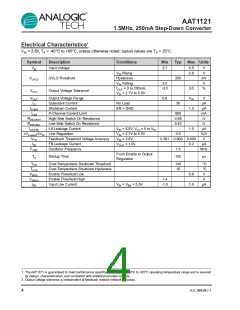
Absolute Maximum Ratings
Symbol
Description
Value
Units
VIN
VLX
VOUT
VEN
TJ
Input Voltage and Bias Power to GND
LX to GND
FB to GND
6.0
V
V
V
V
°C
°C
-0.3 to VIN + 0.3
-0.3 to VIN + 0.3
-0.3 to 6.0
-40 to 150
300
EN to GND
Operating Junction Temperature Range
Maximum Soldering Temperature (at leads, 10 sec)
TLEAD
Thermal Information
Symbol
Description
Value
Units
PD
θJA
Maximum Power Dissipation
Thermal Resistance
2
50
W
°C/W
2
1. Stresses above those listed in Absolute Maximum Ratings may cause permanent damage to the device. Functional operation at condi-
tions other than the operating conditions specified is not implied. Only one Absolute Maximum Rating should be applied at any one time.
2. Mounted on an FR4 board.
1121.2007.03.1.2
3

 ANALOGICTECH [ ADVANCED ANALOGIC TECHNOLOGIES ]