AAT1121
1.5MHz, 250mA Step-Down Converter
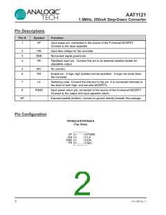
Pin Descriptions
Pin #
Symbol
Function
1
VP
Input power pin; connected to the source of the P-channel MOSFET.
Connect to the input capacitor.
2
3
4
VIN
GND
FB
Input bias voltage for the converter.
Non-power signal ground pin.
Feedback input pin. Connect this pin to an external resistive divider for
adjustable output.
5
6
N/C
EN
No connect.
Enable pin. A logic high enables normal operation. A logic low shuts down
the converter.
7
8
LX
Switching node. Connect the inductor to this pin. It is connected internally to
the drain of both high- and low-side MOSFETs.
PGND
Input power return pin; connected to the source of the N-channel MOSFET.
Connect to the output and input capacitor return.
EP
Exposed paddle (bottom): connect to ground directly beneath the package.
Pin Configuration
TDFN22-8/STDFN22-8
(Top View)
1
2
3
4
8
7
6
5
VP
VIN
GND
FB
PGND
LX
EN
N/C
2
1121.2007.03.1.2

 ANALOGICTECH [ ADVANCED ANALOGIC TECHNOLOGIES ]