AS8221
Data Sheet - Absolute Maximum Ratings
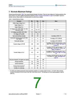
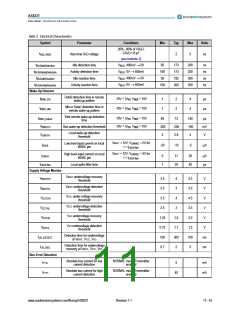
5 Absolute Maximum Ratings
Stresses beyond those listed in Table 2 may cause permanent damage to the device. These are stress ratings only. Functional operation of the
device at these or any other conditions beyond those indicated in Section 6 Electrical Characteristics on page 8 is not implied. Exposure to
absolute maximum rating conditions for extended periods may affect device reliability.
Table 2. Absolute Maximum Ratings
Parameter
Min
-0.3
-0.3
-0.3
Max
+50
Units
Notes
Battery Supply Voltage (VBAT)
Supply Voltage (VCC)
Supply Voltage (VIO)
V
V
V
+7.0
+7.0
DC Voltage at EN, STBN, ERRN, TxD, RxD,
TxEN, BGE, RxEN
-0.3
VIO + 0.3
V
VIO < VCC
DC Voltage on pin WAKE, INH1, INH2
DC Voltage at BP and BM
-0.3
-40
VBAT + 0.3
+50
V
Input current (latchup immunity)
-100
100
mA
According to JEDEC 78
According to AEC-Q100-002
According to AEC-Q100-002
Electrostatic discharge at bus lines BP, BM,
-4
-2
+4
+2
kV
kV
VBAT, WAKE
Electrostatic discharge
According to ISO7637 part3 test pulses a and b;
class C; RL=45 Ω, CL= 100 pF; (see Figure 18
on page 33).
Transient voltage on BP, BM
-200
-200
+6.5
+200
+200
+50
V
V
V
According to ISO7637 part2 test pulses 1, 2, 3a
and 3b; class C; RL=45 Ω, CL= 100 pF; (see
Figure 18 on page 33).
According to ISO7637 part2 test pulse 4; class C;
RL=45 Ω, CL= 100 pF; (see Figure 18 on page
33).
Transient voltage on VBAT
According to ISO7637 part2 test pulse 5b; class
C; RL=45 Ω, CL= 100 pF; (see Figure 18 on
page 33).
+50
Total power dissipation (all supplies and outputs)
Storage temperature
150
+150
+150
mW
ºC
-55
-40
Junction temperature
ºC
Package body temperature1
Humidity non-condensing
250
85
ºC
%
5
1. The reflow peak soldering temperature (body temperature) specified is in accordance with IPC/JEDEC J-STD-020C “Moisture/Reflow
Sensitivity Classification for Non-Hermetic Solid State Surface Mount Devices”. The lead finish for Pb-free leaded packages is matte tin
(100% Sn).
www.austriamicrosystems.com/flexray/AS8221
Revision 1.1
7 - 43

 AMSCO [ AMS(艾迈斯) ]