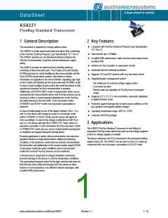
AS8221
Data Sheet - Pin Assignments
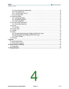
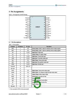
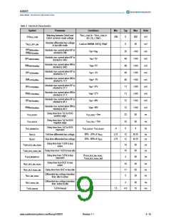
4 Pin Assignments
Figure 2. Pin Assignments SSOP20 Package
1
2
3
4
5
6
7
8
n.u
INH2
INH1
20
19
VCC
BP
EN
VIO
TxD
18
17
16
BM
GND
AS8221
WAKE
VBAT
ERRN
RxEN
n.u
TxEN
RxD
BGE
15
14
13
STBN
9
12
11
10
Reserved
4.1 Pin Descriptions
Table 1. Pin Descriptions
Pin Name
INH2
INH1
EN
Pin Number
Pin Type
AIO
Description
Analog Output. Inhibit 2 output for switching external voltage regulator
Analog Output. Inhibit 1 output for switching external voltage regulator
Digital Input. Enable input
1
2
3
4
5
6
7
8
9
AIO
DI_PD
S
Supply Voltage. I/O supply voltage
VIO
Digital Input. Transmit data input
TxD
DI_PD
DI_PU
DO
Digital Input. Transmitter enable input
TxEN
RxD
Digital Output. Receive data output
Digital Input. Bus guardian enable input
BGE
STBN
DI_PD
DI_PD
Digital Input. Standby input
1
Reserved
10
A/DIO_PD
Not used
RxEN
ERRN
VBAT
WAKE
GND
11
12
13
14
15
16
17
18
19
20
Digital Output. Receive data enable output
Digital Output. Error diagnosis output and wake status output
Supply Voltage. Battery supply voltage
Analog Input. Local wake-up input
Ground
DO
DO
S
AIO
S
Analog Input/Output. Bus line Minus
Analog Input/Output. Bus line Plus
Supply voltage.
BM
AIO
AIO
S
BP
VCC
Not used
1. To be connected to GND or to be unconnected
www.austriamicrosystems.com/flexray/AS8221
Revision 1.1
5 - 43

 AMSCO [ AMS(艾迈斯) ]